Semiconductor integrated circuit device

Inactive Publication Date: 2010-05-20
RENESAS ELECTRONICS CORP
View PDF13 Cites 27 Cited by
  • Summary
  • Abstract
  • Description
  • Claims
  • Application Information

AI Technical Summary

Benefits of technology

[0021](3) From the above points (1) and (2), without deteriorating the performance in a semi

Problems solved by technology

Moreover, the resistance in a wiring network becomes high, and there i

Method used


Image

  • Semiconductor integrated circuit device
  • Semiconductor integrated circuit device
  • Semiconductor integrated circuit device

Examples


Example

First Embodiment

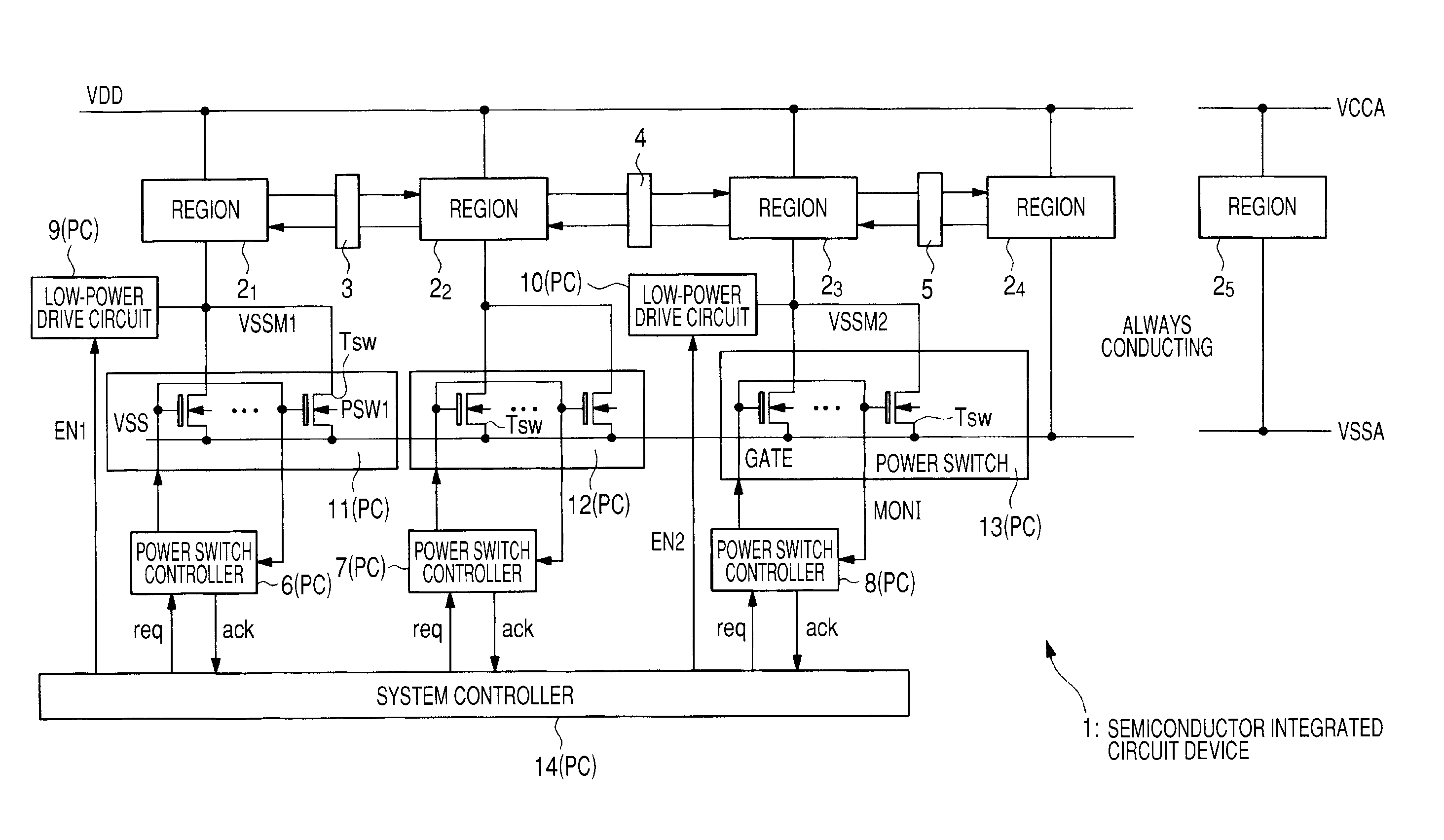
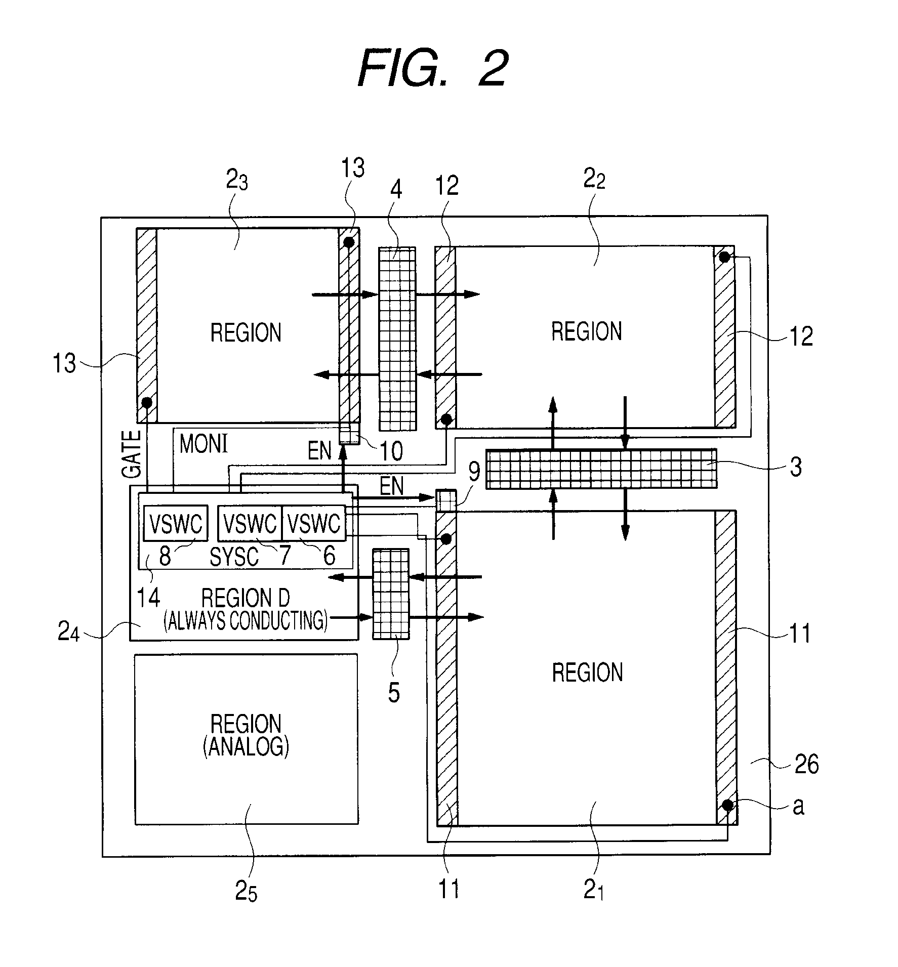
[0045]FIG. 1 is an explanatory diagram showing a configuration example of a semiconductor integrated circuit device according to a first embodiment of the present invention. FIG. 2 is a layout diagram showing an example of a chip layout of the semiconductor integrated circuit device of FIG. 1. FIGS. 3A to 3D are explanatory diagrams showing layout examples in a low-power drive circuit provided for the semiconductor integrated circuit device of FIG. 1. FIG. 4 is an explanatory diagram showing the configuration of a power switch controller provided for the semiconductor integrated circuit device of FIG. 1. FIG. 5 is an explanatory diagram showing an example of voltage control of a virtual reference potential by the power switch controller and the low-power drive circuit provided for the semiconductor integrated circuit device of FIG. 1. FIG. 6 is an explanatory diagram showing another configuration example of the power switch controller according to the first embodimen...

Example

Second Embodiment

[0110]FIG. 8 is an explanatory diagram showing a configuration example of a semiconductor integrated circuit device according to second embodiment of the invention. FIG. 9 is an explanatory diagram showing an example of a mounting image of the semiconductor integrated circuit device of FIG. 8 and a low-power drive circuit.

[0111]The second embodiment relates to a configuration obtained by eliminating the low-power drive circuits 9 and 10 from the configuration of the semiconductor integrated circuit device 1 (FIG. 1) of the first embodiment. The low-power drive circuit 9 for varying the voltage of the virtual reference potential VSSM of the region 21 is externally coupled to the semiconductor integrated circuit device 1.

[0112]As shown in FIG. 8, the semiconductor integrated circuit device 1 is provided with a power supply terminal Pvdd, a ground terminal Pvss, and a second ground terminal Pvssm. The low-power drive circuit 9 is coupled to a ring-shaped virtual refere...

Example

Third Embodiment

[0122]FIG. 10 is a top view of a semiconductor integrated circuit device according to a third embodiment of the invention. FIG. 11 is a cross section taken along A-B of FIG. 10. FIG. 12 is a cross section showing an example of a semiconductor chip provided for the semiconductor integrated circuit device of FIG. 10.

[0123]In the forgoing second embodiment, an example of coupling the low-power drive circuit 9 on the outside to the semiconductor integrated circuit device 1 has been described. In the third embodiment, an example of a semiconductor integrated circuit device 1a obtained by housing the low-power drive circuit 9 and the semiconductor integrated circuit device 1 in a single package will be described.

[0124]FIG. 10 is a top view of the semiconductor integrated circuit device 1a, and FIG. 11 is a cross section taken along A-B of FIG. 10.

[0125]The semiconductor integrated circuit device 1a is a system-in-package having the semiconductor chip 26 configuring the sem...


PUM


Abstract

The present invention is directed to perform fine low-voltage control without largely increasing the circuit layout area in a low-power consumption structure. In the case of shifting a region to a low-speed mode, a system controller outputs a request signal and an enable signal to a power switch controller and a low-power drive circuit, respectively, to turn off a power switch and to perform a control so that the voltage level of a virtual reference potential becomes about 0.2 V to about 0.3V. The region operates on voltages between a power supply voltage and a virtual reference potential, so that it is controlled in the low-speed mode.

Description

CROSS-REFERENCE TO RELATED APPLICATIONS[0001]The disclosure of Japanese Patent Application No. 2008-291929 filed on Nov. 14, 2008 including the specification, drawings and abstract is incorporated herein by reference in its entirety.BACKGROUND OF THE INVENTION[0002]The present invention relates to a technique for lowering power consumption of a semiconductor integrated circuit device and, more particularly, to a technique effective to high-precision reduction of power consumption in a semiconductor integrated circuit device having a plurality of power supply regions in which low-power-consumption control is performed.[0003]In recent years, a demand for lower power consumption is increasing. As a technique for reducing power consumption, for example, there is known a technique of dividing a core power region (for example, by logic blocks), controlling the on / off state of a power supply by the divided regions and, in the case of a low-speed operation or the like, controlling a power s...

Claims


Application Information

Patent Timeline
IPC IPC(8): G05F1/10
CPCG06F1/3203G06F1/3287H01L27/0207H01L27/088H03K19/0016Y02B60/32H01L2224/48091Y02B60/1282H01L2924/13091H01L2924/00014Y02D10/00Y02D30/50H01L2924/00
Inventor SASAKI, TOSHIOFUKUOKA, KAZUKIMORI, RYOYASU, YOSHIHIKO
Owner RENESAS ELECTRONICS CORP
Why Eureka
Try Eureka