
Image reading and writing using a complex two-dimensional interlace scheme

a two-dimensional interlace scheme and image reading technology, applied in the field of writing or reading patterns on the surface, can solve the problem that the output does not scale with the array size, and achieve the effect of improving throughpu

Active Publication Date: 2010-05-27
MICRONIC LASER SYST AB
View PDF11 Cites 35 Cited by
  • Summary
  • Abstract
  • Description
  • Claims
  • Application Information

AI Technical Summary

Benefits of technology

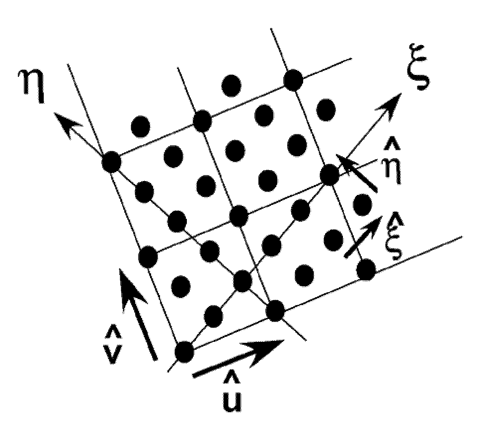
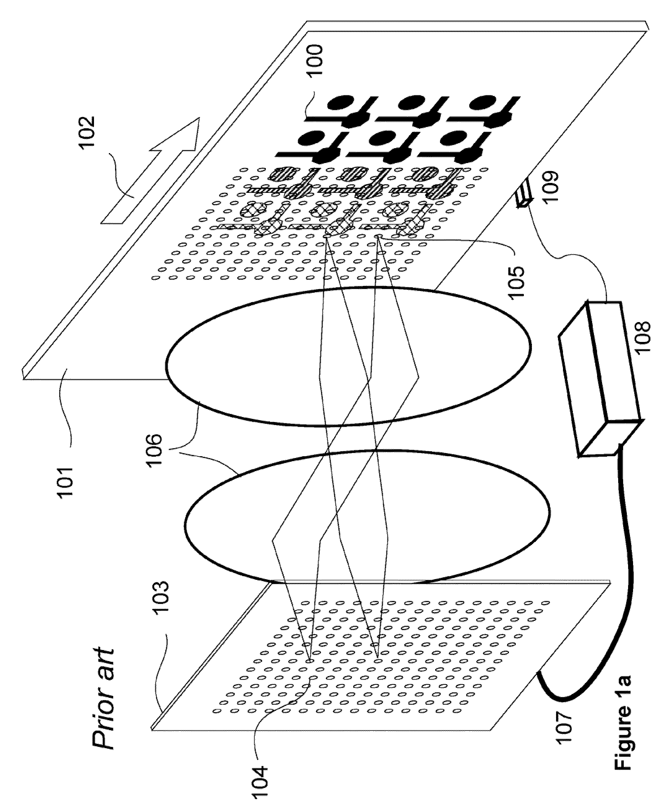
[0018]The technology disclosed relates to writing or reading a pattern on a surface, such as in microlithography or inspection of mircrolithographic patterns. In particular, Applicant discloses systems recording or reading images by scanning sparse 2D point arrays or grids across the surface, e.g., multiple optical, electron or particle beams modulated in parallel. The scanning and repeated reading or writing creates a dense pixel or spot grid on the workpiece. The grid may be created by various arrays: arrays of light sources, e.g., laser or LED arrays, by lenslet arrays where each lenslet has its own modulator, by aperture plates for particle beams, or arrays of near-field emitters or mechanical probes. For reading systems, the point grid may be created by a sparse point matrix illumination and / or a detector array where each detector element sees only one spot. The idea behind the use of large arrays is to improve throughput. However, the throughput does not scale with the array size, since above a certain size of arrays, previously known schemes fall into their own tracks and start repeating the same data over and over again. This application discloses methods to scan workpieces with large arrays while preserving the scaling of throughput proportional to array size, even for very large arrays, in fact essentially without limits. This is done by first determineing a necessary density of grid points in the read or written image, then finding the longest travel per laser pulse, or similar, which produces this density of points when the array staverses the workpiece. The Applicant has found that by rotation of the array vs. the direction of travel and minor adjustment of the distance between laser pulses, it is possible to find a combination of angle and distance which creates the desired density while using all or almost all of the elements in the array, and has deviced methods to find such combinations. Furthermore there are several combinations using essentially the full capacity of the array, and these combination may have different properties in terms of grid orientation, uniformity and suppression of systematic errors.

Problems solved by technology

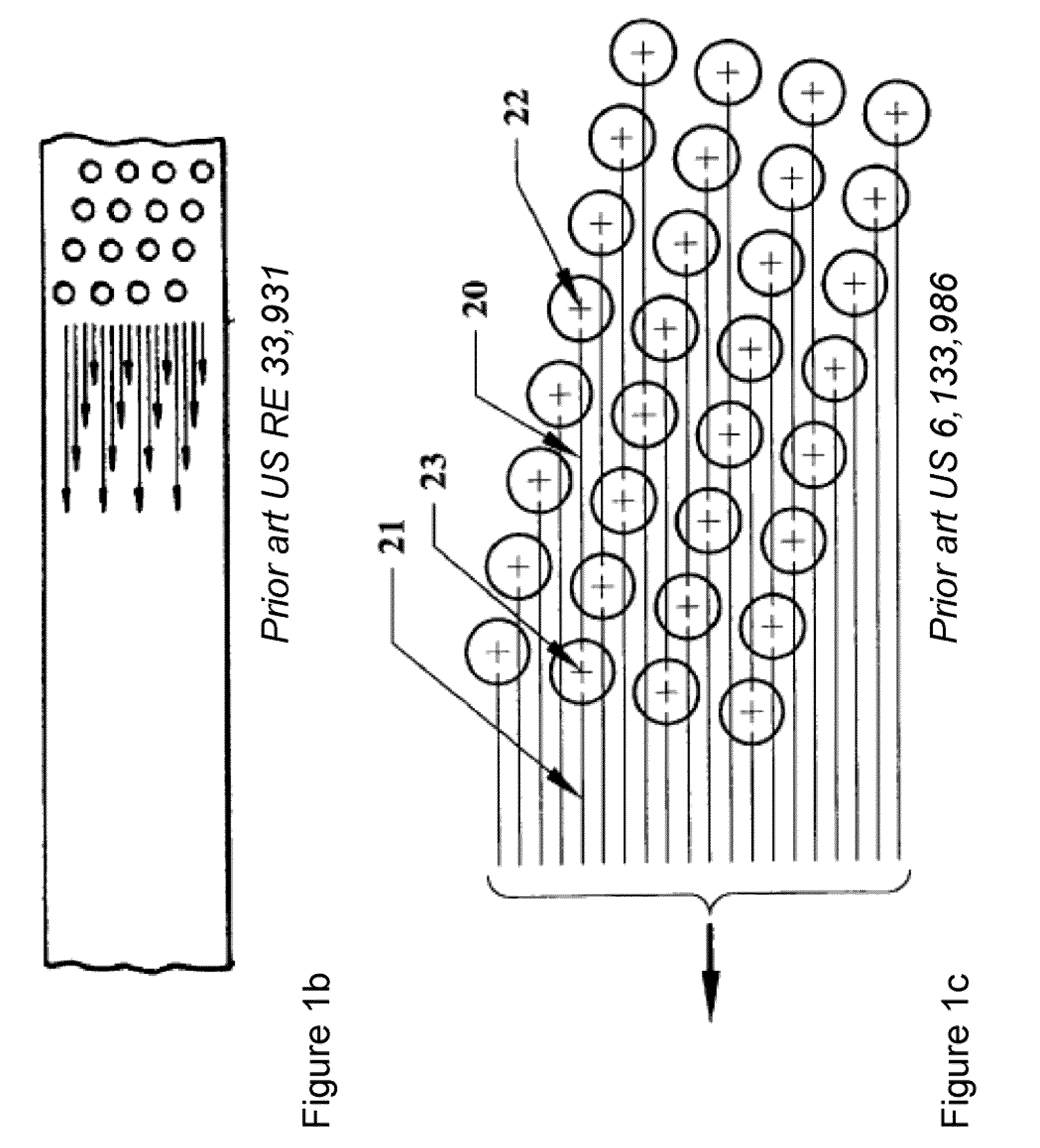
However, the throughput does not scale with the array size, since above a certain size of arrays, previously known schemes fall into their own tracks and start repeating the same data over and over again.

Method used


Image

  • Image reading and writing using a complex two-dimensional interlace scheme
  • Image reading and writing using a complex two-dimensional interlace scheme
  • Image reading and writing using a complex two-dimensional interlace scheme

Examples


writer embodiment

Optical Direct Writer Embodiment

[0099]In this section, we disclose an embodiment of an optical direct writer for writing LCD backplanes with an optical resolution of 3.5 microns and a minimum feature size of 5 microns. The resist has a sensitivity of 30 mJ / cm2.

[0100]The modulator array in the preferred embodiment is a Texas Instruments HDTV DLP (Digital Light Processing) chip with 1920×1080 binary mirrors and max frame rate of 23 kHz. The mirror to mirror pitch on the chip is 10.8 microns. The chip is oriented as in FIG. 2 with the translation vector being along the shortest axis, but tilted at an angle. The long axis of the chip defines the stripe width and the entire width can be used. In the direction of translation, the utilization of the chip depends on the interlace parameters. A prefered set of parameters is ncell=481, nu=9, nv=9, nskip=29 and to the basic fractional translation vector a vector (0, 1) cells is added. This makes 98% of the mirrors contribute to the throughput,...


PUM

PropertyMeasurementUnit
Fractionaaaaaaaaaa
Fractionaaaaaaaaaa
Fractionaaaaaaaaaa

Abstract

The current invention relates to writing or reading a pattern on a surface, such as in microlithography or inspection of mircrolithographic patterns. In particular, Applicant discloses systems recording or reading images by scanning sparse 2D point arrays or grids across the surface, e.g., multiple optical, electron or particle beams modulated in parallel. The scanning and repeated reading or writing creates a dense pixel or spot grid on the workpiece. The grid may be created by various arrays: arrays of light sources, e.g., laser or LED arrays, by lenslet arrays where each lenslet has its own modulator, by aperture plates for particle beams, or arrays of near-field emitters or mechanical probes. For reading systems, the point grid may be created by a sparse point matrix illumination and / or a detector array where each detector element sees only one spot. The idea behind the use of large arrays is to improve throughput. However, the throughput does not scale with the array size, since above a certain size of arrays, previously known schemes fall into in their own tracks and start repeating the same data over and over again. This application discloses methods to scan workpieces with large arrays while preserving the scaling of throughput proportional to array size, even for very large arrays, in fact essentially without limits.

Description

RELATED APPLICATION[0001]This application is related to and claims the benefit of U.S. Provisional Patent Application No. 61 / 118,299, entitled, “Image Reading and Writing Using a Complex Two-Dimensional Interlace Scheme,” filed on Nov. 26, 2008. The related application is incorporated by reference.BACKGROUND OF THE INVENTION[0002]The technology disclosed relates to writing or reading a pattern on a surface, such as in microlithography or inspection of mircrolithographic patterns. In particular, Applicant discloses systems recording or reading images by scanning sparse 2D point arrays or grids across the surface, e.g., multiple optical, electron or particle beams modulated in parallel. The scanning and repeated reading or writing creates a dense pixel or spot grid on the workpiece. The grid may be created by various arrays: arrays of light sources, e.g., laser or LED arrays, by lenslet arrays where each lenslet has its own modulator, by aperture plates for particle beams, or arrays o...

Claims


Application Information

Patent Timeline
IPC IPC(8): B29C35/08
CPCG02B3/0037G02B5/003G06K17/00G03F7/70291G02B26/0833G03F7/70041G03F7/70508
Inventor SANDSTROM, TORBJORN
Owner MICRONIC LASER SYST AB
Learn More