Anisotropic conductive connector, probe member and wafer inspection system

Active Publication Date: 2010-05-27
ISC CO LTD
View PDF9 Cites 8 Cited by
  • Summary
  • Abstract
  • Description
  • Claims
  • Application Information

AI Technical Summary

Benefits of technology

[0044]In the anisotropic conductive connector according to the third invention, since the connection conductive parts of the elastic anisotropic conductive films disposed in the peripheral area of the frame plate have a content of the conductive particles higher than that of the connection conductive parts of the elastic anisotropic conductive films disposed in the center area of the frame plate, a decrease in conductivity of the connection conductive parts disposed in the peripheral area of the frame plate can be inhibited even when the anisotropic conductive connector is repeatedly used many times over. Therefore, the anisotropic conductive connector has a long service life.
[0045]In the anisotropic conductive connector according to the fourth invention, since the connection conductive parts of the elastic anisotropic conductive films disposed in the peripheral area of the frame plate have a horizontal cross-sectional area larger than that of the connection conductive parts of the elastic anisotropic conductive films disposed in the center area of the frame plate, the connection conductive parts of the elastic anisotropic conductive films disposed in a peripheral area of the frame plate have higher strength as compared with the connection conductive parts of the elastic anisotropic conductive films disposed in the center area of the frame plate and since the connection conductive parts having a large cross-sectional area have a lower electrical resistance, a decrease in conductivity of the connection conductive parts disposed in the peripheral area of the frame plate can be inhibited even when the anisotropic conductive connector is repeatedly used many times over. Therefore, the anisotropic conductive connector has a long service life. Further, the connection conductive parts of the elastic anisotropic conductive films disposed in the center area of the frame plate are sufficiently compressed by a lower pressing force due to small cross-sectional area thereof so that uniform conductivity is achieved in all of the connection conductive parts even when the anisotropic conductive connector is one having a large area.

Problems solved by technology

On the other hand, in the burn-in test, since the inspection target integrated circuit devices are minute and have poor handling capability, a long time is required to conduct electrical inspection of a number of integrated circuit devices individually, and thus the inspection cost is considerably high.
However, when the inspection target wafer has a diameter as large as 12 inches or more and the number of inspection target electrodes is 10,000 or more, particularly 20,000 or more, for example, wherein arrangement pitch of the inspection target electrodes of each integrated circuit is extremely small, the following problems are encountered when the above anisotropic conductive connector as a probe member is used for the probe test or WLBI test.
However, when such an anisotropic conductive elastomer sheet is compressed by the wafer and the inspection circuit board, the conductive parts disposed in a peripheral area of the anisotropic conductive elastomer sheet may be sufficiently compressed, but the conductive parts disposed in a center area of the anisotropic conductive elastomer sheet are not sufficiently compressed.
Therefore, conductivity of the conductive parts becomes non-uniform.
In this case, a problem is encountered in that, since an excessive pressing force is applied to the conductive parts disposed in the peripheral area of the anisotropic conductive elastomer sheet, the conductive parts disposed in the peripheral area break and their conductivity decreases when used repeatedly, with a result that a long service life thereof could not be availed.

Method used


Image

  • Anisotropic conductive connector, probe member and wafer inspection system
  • Anisotropic conductive connector, probe member and wafer inspection system
  • Anisotropic conductive connector, probe member and wafer inspection system

Examples


Embodiment Construction

[0103]Embodiments of the present invention are described in detail below. Anisotropic conductive connector

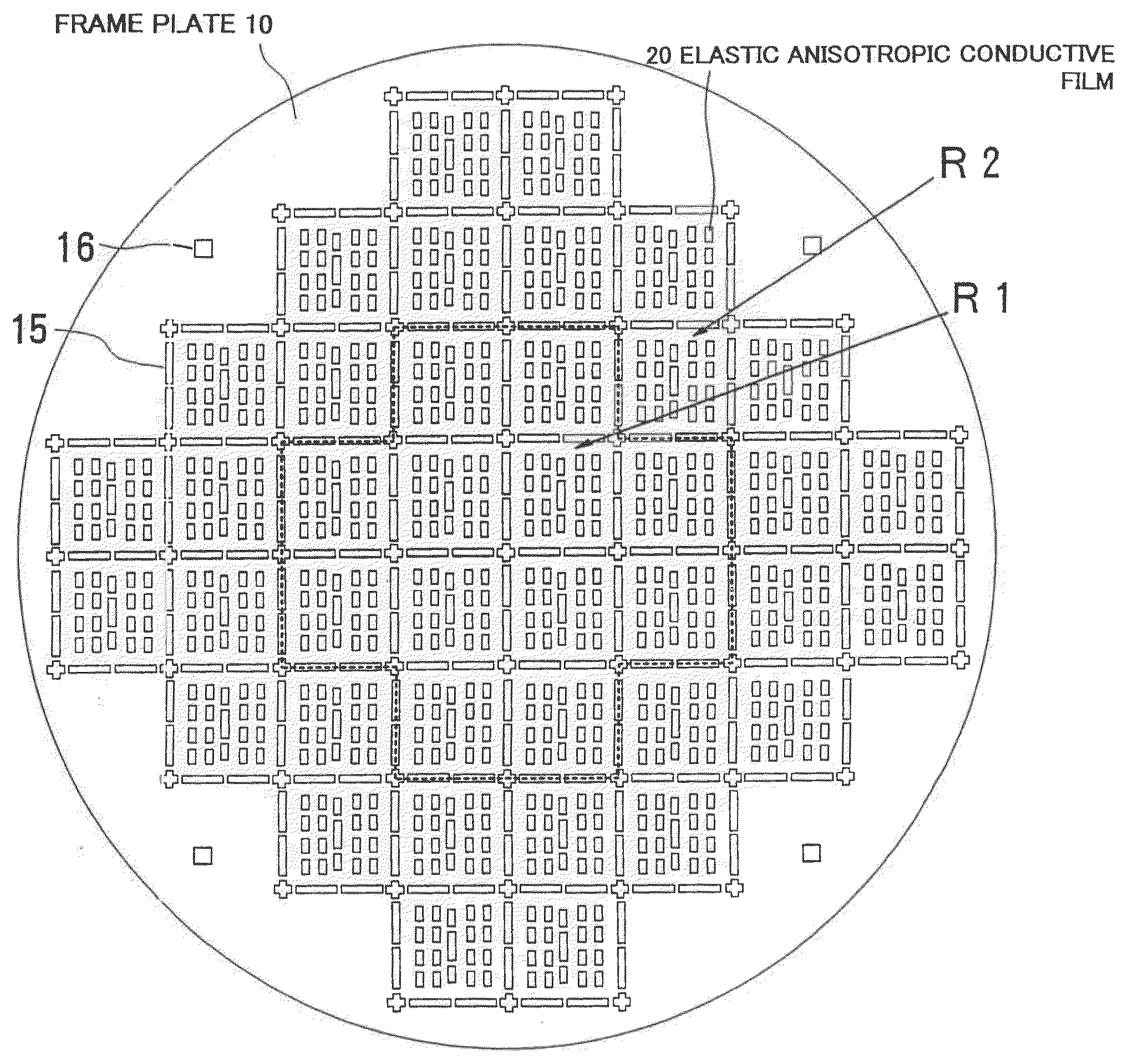
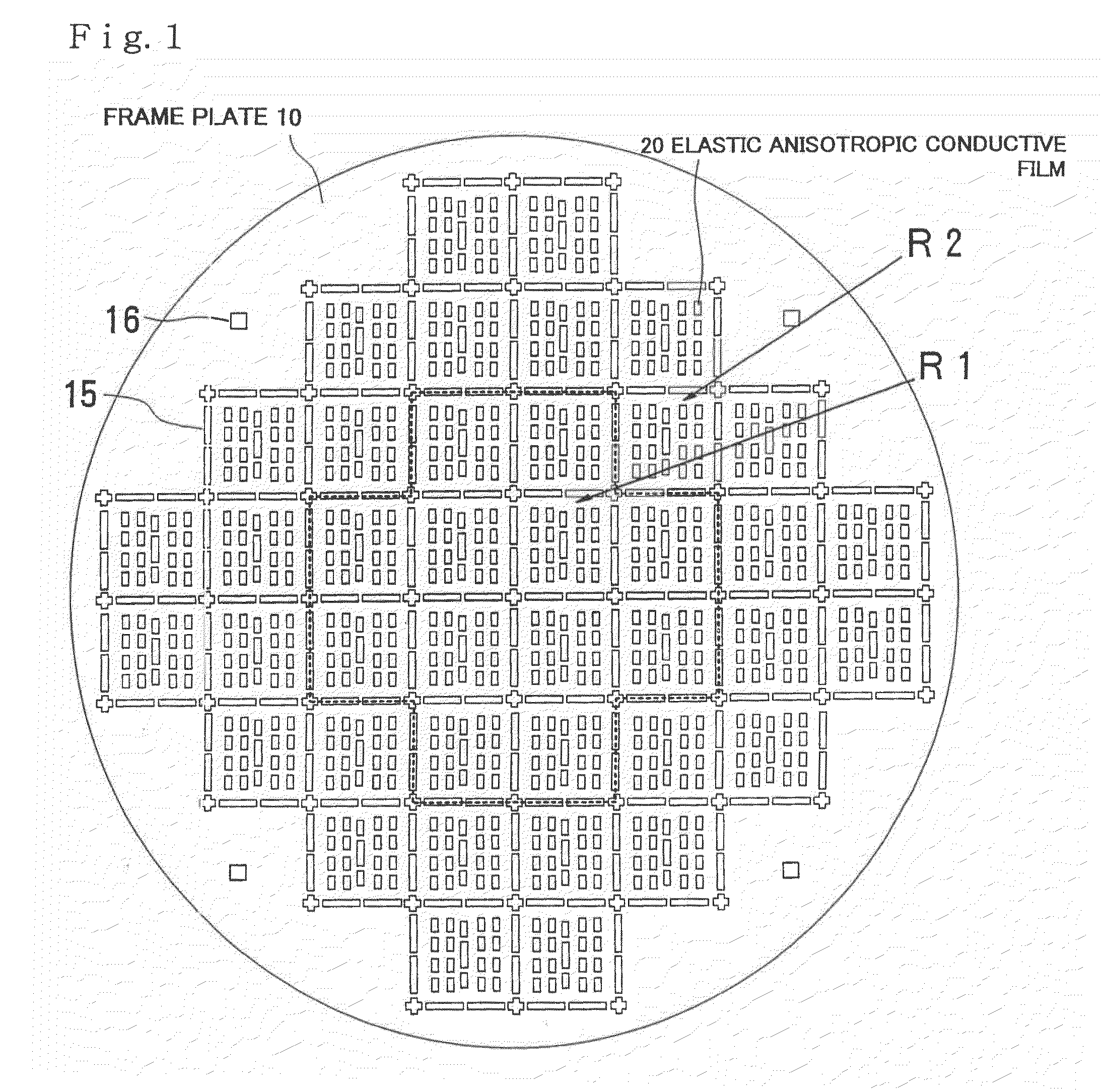
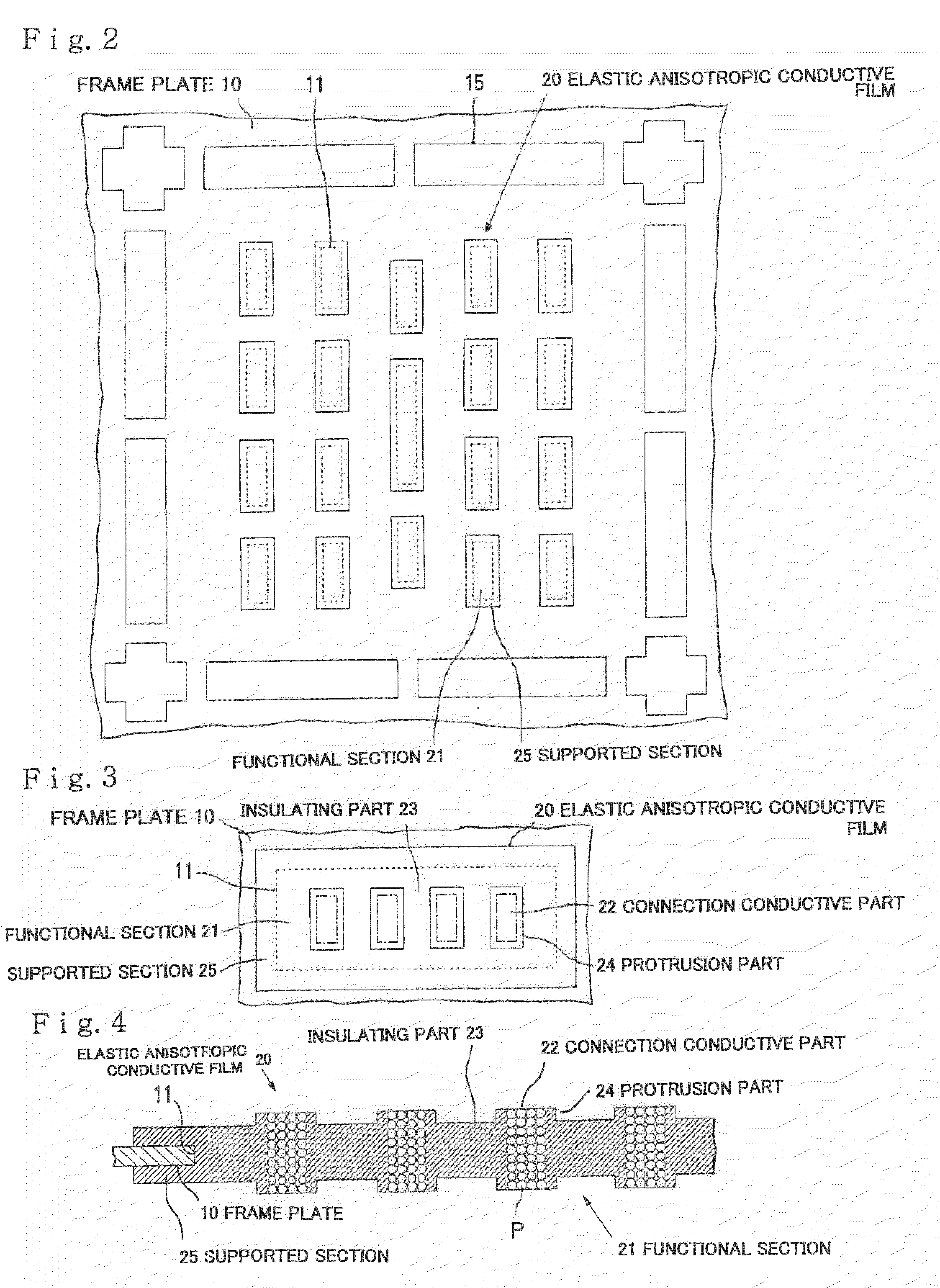
[0104]FIG. 1 is a plan view showing an example of an anisotropic conductive connector according to the present invention, FIG. 2 is a plan view showing, in an enlarged scale, a part of the anisotropic conductive connector shown in FIG. 1, FIG. 3 is a plan view showing, in an enlarged scale, an elastic anisotropic conductive film in the anisotropic conductive connector shown in FIG. 1, and FIG. 4 is a cross-sectional illustration showing, in an enlarged scale, the elastic anisotropic conductive film of the anisotropic conductive connector shown in FIG. 1.

[0105]The anisotropic conductive connector shown in FIG. 1 is used to conduct an electrical inspection of each of a plurality of integrated circuits formed on a wafer in a state of the wafer, for example. As shown in FIG. 2, the anisotropic conductive connector includes a frame plate 10, in which a plurality of anisotropic conduc...


PUM


Abstract

Provided is an anisotropic conductive connector and a prove member, each of which ensures that all of the conductive parts exhibit uniform conductivity when a pressing force is applied, even when the inspection target wafer has a large area and total number of inspection target electrodes of integrated circuits is 10,000 or more, and a wafer inspection system including the probe member. The anisotropic conductive connector includes a frame plate in which a plurality of anisotropic conductive film placement holes are formed, and elastic anisotropic conductive films respectively disposed in the anisotropic conductive film placement holes in the frame plate and supported by a peripheral part of the frame plate around the corresponding anisotropic conductive film placement hole, each of the elastic anisotropic conductive films includes a plurality of connection conductive parts each extending in a thicknesswise direction of the elastic anisotropic conductive film, being disposed corresponding to a connection target electrode, and comprising an elastic polymer substance and magnetic conductive particles densely contained in the elastic polymer substance; and an insulating part that insulates the connection conductive parts to one another, and the connection conductive parts of the elastic anisotropic conductive films disposed in a peripheral area of the frame plate having a thickness smaller than that of the connection conductive parts of the elastic anisotropic conductive films disposed in a center area of the frame plate.

Description

TECHNICAL FIELD[0001]The present invention relates to an anisotropic conductive connector that is used to conduct an electrical inspection of a plurality of integrated circuits formed on a wafer in a state of the wafer, a probe member including the anisotropic conductive connector, and a wafer inspection system including the probe member. More particularly, the present invention relates to an anisotropic conductive connector that is suitably used to conduct an electrical inspection of a plurality of integrated circuits formed on a wafer when the wafer has a diameter of 12 inches or more and the total number of inspection target electrodes of the integrated circuits formed on the wafer is 10,000 or more, for example, a probe member including the anisotropic conductive connector, and a wafer inspection system including the probe member.BACKGROUND ART[0002]Generally, in a production process of semiconductor integrated circuit devices, a number of integrated circuits are formed on a waf...

Claims


Application Information

Patent Timeline
IPC IPC(8): G01R31/02H01R4/58
CPCG01R1/0491H01R13/2414G01R1/0735G01R1/073H01B5/16H01R11/01
Inventor NAOI, MASAYAFUJIYAMA, HITOSHIMIURA, ICHIHIRO
Owner ISC CO LTD
Why Eureka
Try Eureka