Tolerant buffer circuit and interface
- Summary
- Abstract
- Description
- Claims
- Application Information
AI Technical Summary
Benefits of technology
Problems solved by technology
Method used
Image

Examples
embodiment 1
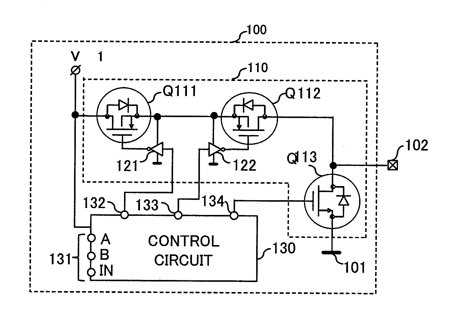
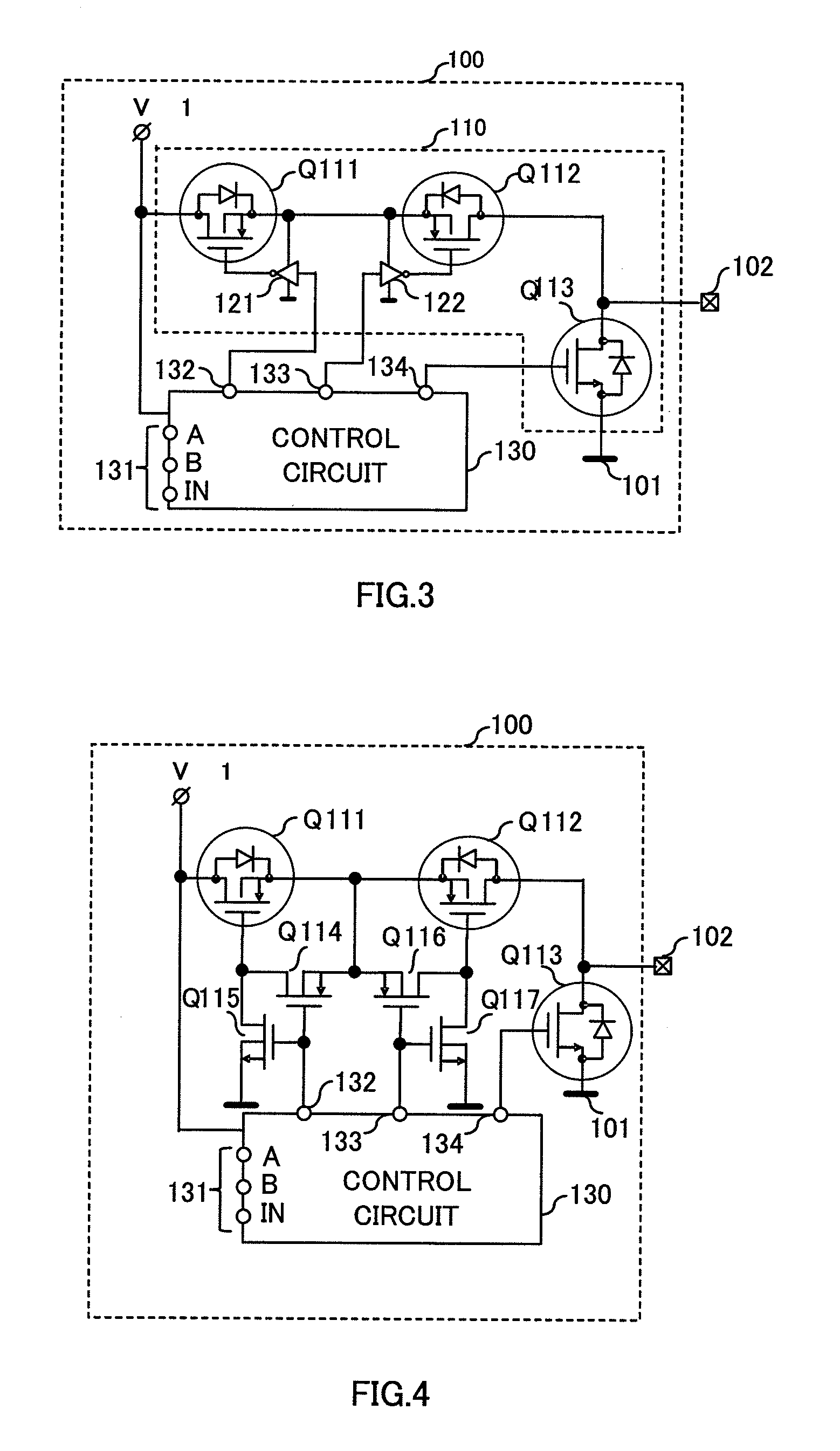
[0030]FIG. 3 is a circuit diagram showing a configuration of a tolerant buffer circuit according to Embodiment 1 of the present invention. This embodiment is an example of application to a tolerant buffer circuit incorporated in an output interface.
[0031]As shown in FIG. 3, tolerant buffer circuit 100 is configured by means of output circuit 110, control circuit 130 that controls output circuit 110, power supply terminal VDD1, ground terminal 101, and output terminal 102.
[0032]Output circuit 110 is configured by means of P-channel MOS transistors Q111 and Q112 that are connected in series and that share a source between power supply terminal VDD1 and output terminal 102, N-channel MOS transistor Q113 connected between output terminal 102 and ground terminal 101, inverter 121 output-connected to the gate of P-channel MOS transistor Q111, and inverter 122 output-connected to the gate of P-channel MOS transistor Q112.
[0033]Control circuit 130 is provided with input terminals 131 compri...
embodiment 2
[0083]Embodiment 2 is an example of application of tolerant buffer circuit 100 to a UART interface.
[0084]FIG. 7 is a block diagram of a UART interface having a tolerant buffer circuit according to Embodiment 2 of the present invention. Configuration parts that are identical in FIG. 3 and FIG. 4 are assigned the same reference codes, and duplicate descriptions are omitted here.
[0085]As shown in FIG. 7, UART interface 200 is configured by means of CPU 210, register 220, and tolerant buffer circuit 100 having output circuit 110 and control circuit 130. External system circuit 230, an external device, is connected to tolerant buffer circuit 100.
[0086]UART interface 200 incorporating tolerant buffer circuit 100 is an interface configured by means of a receiver (RX) section that receives a signal from external system circuit 230, and a transmitter (TX) section that transmits a signal from CPU 210 to external system circuit 230. FIG. 7 shows the interface of the transmitter (TX) section th...
embodiment 3
[0099]Embodiment 3 is an example in which a plurality of UART interfaces and / or interfaces to external system devices are provided.
[0100]FIG. 8 is a peripheral configuration block diagram including tolerant buffer circuits according to Embodiment 3 of the present invention.
[0101]As shown in FIG. 8, output interface 300 is configured by means of CPU 310, register 320, and plurality of tolerant buffer circuits 100A, 100B, and 100C. External system circuits 330, 340, and 350 are connected to tolerant buffer circuits 100A, 100B, and 100C respectively.
[0102]Tolerant buffer circuits 100A, 100B, and 100C have the same kind of configuration as tolerant buffer circuit 100 shown in FIG. 3, FIG. 4, and FIG. 7. Tolerant buffer circuits 100A, 100B, and 100C are provided with input terminals A1 through A3, B1 through B3, and IN1 through IN3, and output terminals 102A, 102B, and 102C, respectively.
[0103]Signals output from the CPU 310 side are input to input terminals IN1, IN2, and IN3 of tolerant...
PUM
 Abstract
Description
Claims
Application Information
 - R&D Engineer
- R&D Manager
- IP Professional
- Industry Leading Data Capabilities
- Powerful AI technology
- Patent DNA Extraction
Browse by: Latest US Patents, China's latest patents, Technical Efficacy Thesaurus, Application Domain, Technology Topic.
© 2024 PatSnap. All rights reserved.Legal|Privacy policy|Modern Slavery Act Transparency Statement|Sitemap