Method of manufacturing and processing silicon carbide scanning and optical mirrors

a technology of optical mirrors and silicon carbide, which is applied in the direction of coatings, electrical equipment, plasma techniques, etc., can solve the problems of difficult to achieve industrially required flatness with good cost-efficiency, significant cost and time consumption, and difficult to lap and/or polish to achieve industrially required flatness, and achieves faster and cheaper. , the effect of improving the quality of the produ

Inactive Publication Date: 2010-06-03
MERSEN DEUTLAND HLDG
View PDF7 Cites 4 Cited by
  • Summary
  • Abstract
  • Description
  • Claims
  • Application Information

AI Technical Summary

Benefits of technology

[0014]Advantageously, Silicon Carbide is significantly cheaper and faster to manufacture as scanning or optical mirrors when the Silicon Carbide powder is pressed or stamped or isostatically pressed using an engineered stamp or tool and then in this embodiment sintered than when the Silicon Carbide powder is pre-pressed or pre-isostatically pressed and then engineered for example by Computer Numerical Control engineering and then treated or sintered.
[0015]Advantageously, because said layer of material and in this embodiment Silicon bonded to said surface of said Silicon Carbide that will become said reflective surface is significantly easier to lap and / or polish than the raw Silicon Carbide material of said surface without any additional layer material and in this embodiment Silicon said lapping and / or polishing is faster and cheaper.
[0016]Advantageously, because said layer of material and in this embodiment Silicon deposited on or bonded to said surface of said Silicon Carbide that will become said reflective surface is of a significantly finer structure than the raw Silicon Carbide material of said surface without any additional layer of deposited or bonded material said layer of material and in this embodiment Silicon will give a finer surface roughness and / or surface quality after lapping and / or polishing and significantly decrease reflective spatial effects in application when coated with suitable high reflective optical coatings specific to the wavelength or wavelengths that the finished Silicon Carbide scanning or optical mirror will be used to reflect in final application / s.

Problems solved by technology

Firstly, and because Silicon Carbide is a material with an extremely high mechanical hardness it is significantly expensive and time consuming to manufacture as scanning or optical mirrors when the Silicon Carbide powder is pre-pressed or pre-isostatically pressed and then engineered or Computer Numerical Control engineered and then treated or sintered.
Secondly, and because Silicon Carbide is a material with an extremely high mechanical hardness it is significantly expensive and difficult to polish to industrially required flatness with good cost-efficiencies.
Thirdly, because said Silicon Carbide has such said extremely high mechanical hardness, when manufactured for use as for example plano scanning or optical mirrors the surface that will eventually become the reflective surface is required to be produced as flat as possible in preparation for lapping and / or polishing using grinding technology and commonly diamond wheel grinding.
Fourth, because said grinding and commonly diamond wheel grinding can achieve planarity of said example piano Silicon Carbide scanning or optical mirrors depending upon the positional accuracy of said grinding technology said planarity achieved is cost-relative to the said positional accuracy of said grinding technology.
Fifth, because said Silicon Carbide has such said extremely high mechanical hardness the polishing of said example Silicon Carbide scanning or optical mirrors may involve up to four separate lapping and / or polishing stages with greater polishing material / s wear and consumption and greater lapping and / or polishing times.
Seventh, because said surface quality of said Silicon Carbide after lapping and / or polishing will have a surface quality of at best a Ra of 3 micrometers spatial effects may limit the reflective performance of said example plano Silicon Carbide scanning or optical mirrors in applied use after final optical coating.

Method used


Image

  • Method of manufacturing and processing silicon carbide scanning and optical mirrors
  • Method of manufacturing and processing silicon carbide scanning and optical mirrors
  • Method of manufacturing and processing silicon carbide scanning and optical mirrors

Examples


Embodiment Construction

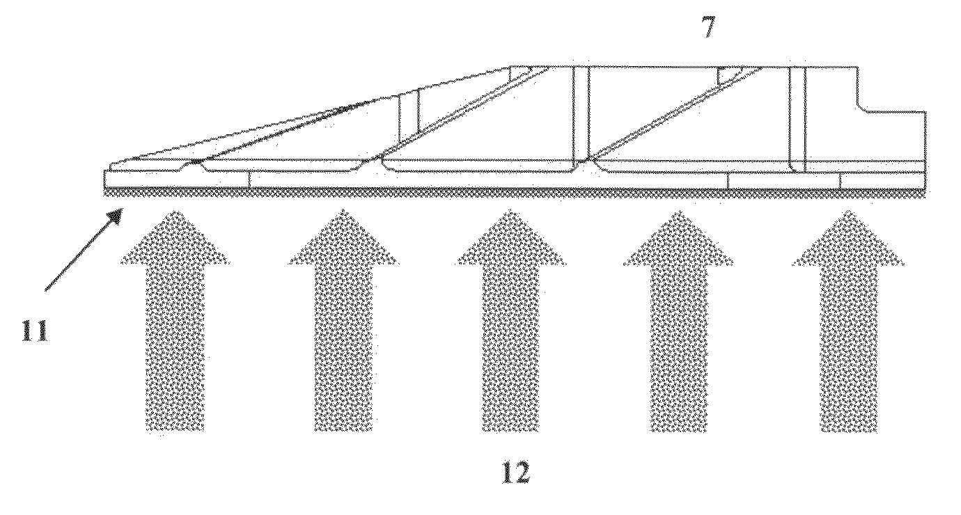
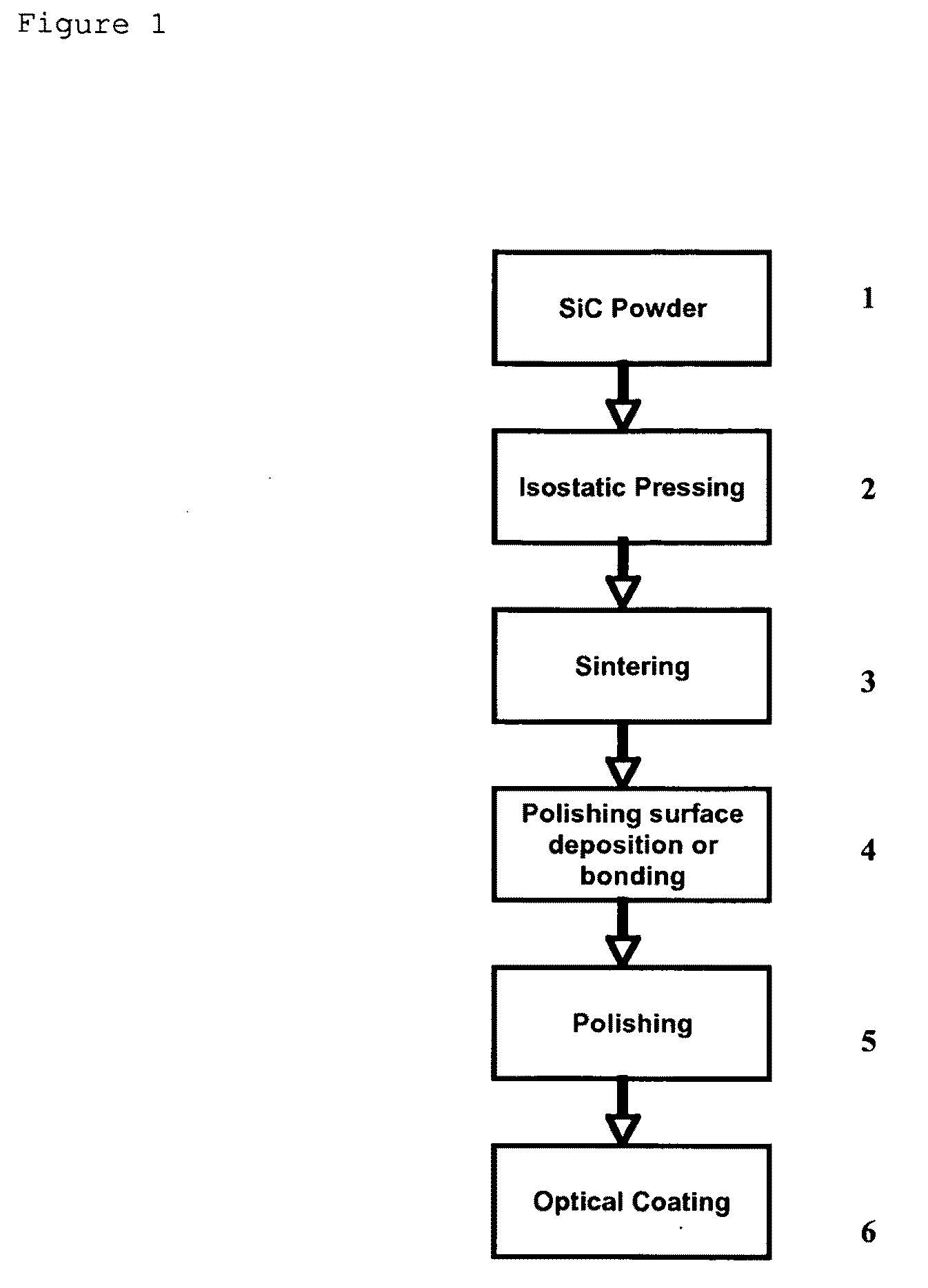
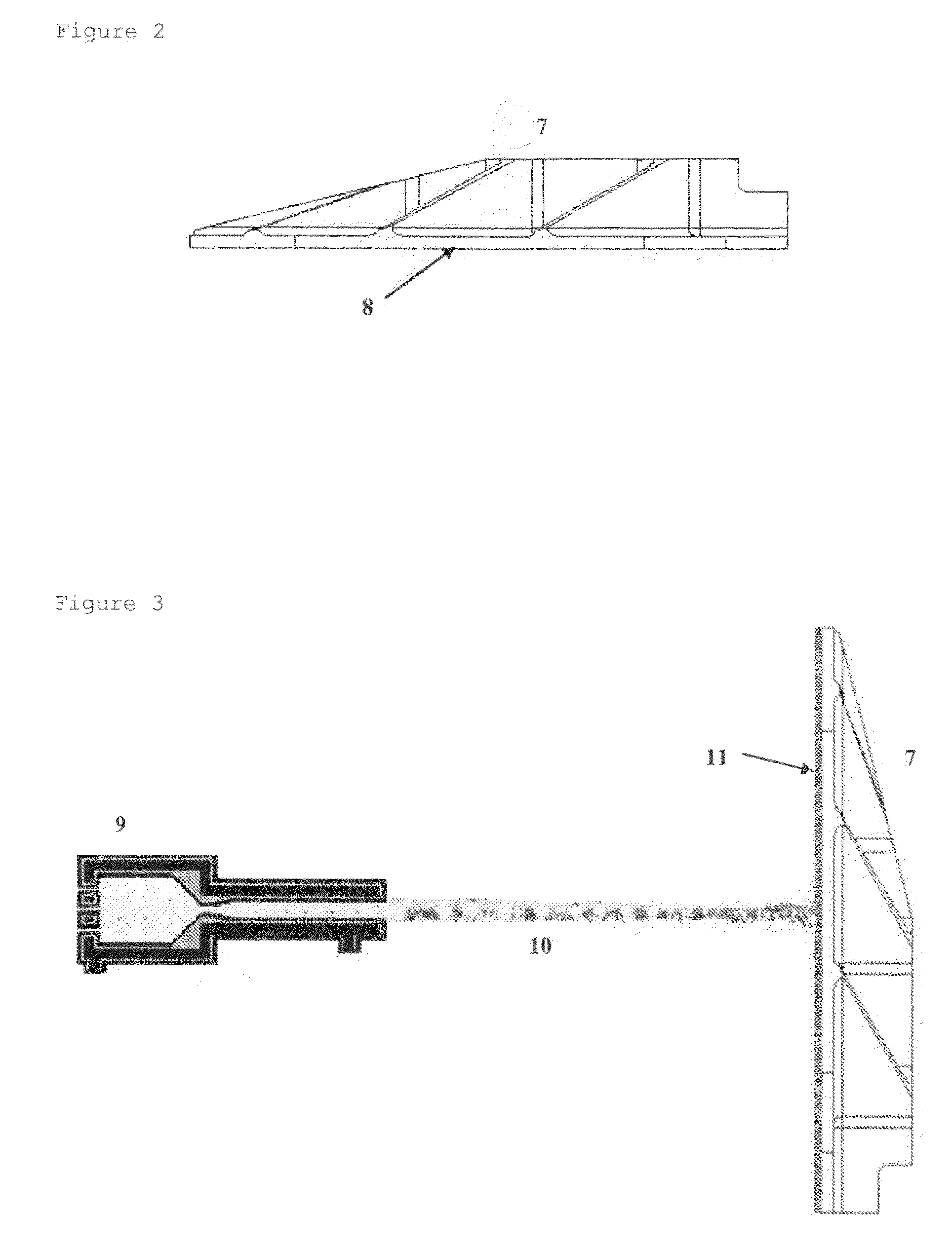
[0023]As depicted in the production process flowchart in FIG. 1, Silicon Carbide powder (1) is pressed or stamped or isostatically pressed (2) using an engineered stamp or tool to form the shape and structure of a scanning or optical mirror which is then in this embodiment sintered (3) to provide a Silicon Carbide scanning or optical mirror with a surface that is the face surface of said scanning or optical mirror that may be then ground using grinding technology and commonly diamond wheel grinding or lapped or polished (not shown) using commonly available lapping and / or polishing technology.

[0024]The Silicon Carbide scanning or optical mirror now with a surface that is the face surface of said scanning or optical mirror ground using grinding technology and commonly diamond wheel grinding or lapped or polished using commonly available lapping and / or polishing technology enters a deposition or bonding process (4) and in this embodiment high velocity Oxygen fuel thermal spray process ...


PUM

PropertyMeasurementUnit
Raaaaaaaaaaa
roughnessaaaaaaaaaa
flatnessaaaaaaaaaa

Abstract

The invention relates to a method of Silicon Carbide scanning or optical mirror production. In order to reduce the costs for manufacturing a scanning or optical mirror, according to the present invention, Silicon Carbide powder is pressed or stamped or isostatically pressed using an engineered stamp or tool to form the shape and structure of a scanning or optical mirror which is then in this embodiment sintered to provide a surface that will become the face surface of said scanning or optical mirror that is then coated or bonded with a suitably thick layer of in this embodiment Silicon material deposited by a thermal spray process onto said face surface of said scanning or optical mirror that is then polished to achieve the desired surface quality and/or roughness and/or flatness and then optical coated using coating technologies and materials to coat said face surface that will then become the reflective surface with suitable high reflective optical coatings specific to the wavelength or wavelengths that the finished Silicon Carbide scanning or optical mirrors will be used to reflect in final application/s.

Description

FIELD OF THE INVENTION[0001]This invention relates to a method of manufacturing and processing of Silicon Carbide scanning or optical mirrors. In addition, the invention relates to the method to achieve low cost production and high quality surface finishes on Silicon Carbide scanning or optical mirrors using available isostatic pressing, sintering and polishing techniques by depositing or bonding an alternative material on said Silicon Carbide scanning or optical mirrors, eg. Silicon, and subsequently using said available polishing techniques to polish said alternative material instead of directly polishing the Silicon Carbide material.BACKGROUND OF THE INVENTION[0002]Traditional Silicon Carbide scanning or optical mirror manufacturing is limited by several factors:[0003]Firstly, and because Silicon Carbide is a material with an extremely high mechanical hardness it is significantly expensive and time consuming to manufacture as scanning or optical mirrors when the Silicon Carbide p...

Claims


Application Information

Patent Timeline
Patent Type & Authority Applications(United States)
IPC IPC(8): C23C4/00C23C4/10C23C4/18C23C4/02G02B5/08
CPCC04B41/009C04B41/5035G02B5/08C04B2111/80C04B41/89C04B41/85C04B41/5096C04B41/5127C04B41/5155C04B41/52C04B41/4527C04B41/53C04B35/565
Inventor HASTINGS, STEPHEN
Owner MERSEN DEUTLAND HLDG
Why Eureka
Try Eureka