Semiconductor device and method of manufacturing the same

a semiconductor and semiconductor technology, applied in the direction of semiconductor devices, radio frequency controlled devices, electrical devices, etc., can solve the problems of reducing charge transfer efficiency and affecting image sensor performance, and achieve the effect of effective implanting many hydrogen ions

Inactive Publication Date: 2010-06-03
DONGBU HITEK CO LTD
View PDF12 Cites 0 Cited by
  • Summary
  • Abstract
  • Description
  • Claims
  • Application Information

AI Technical Summary

Benefits of technology

[0009]An embodiment provides a method of manufacturing a semiconductor device capable of effectively implanting many hydrogen ions into a selected portion of a substrate by using a hydrogen ion implanter in the manufacturing process of the semiconductor device.

Problems solved by technology

The dangling bonds degrade the performance of the image sensor.
Further, the dangling bonds generated when forming the gate insulating layer may reduce charge transfer efficiency because they may serve as a trap that captures electrons during transfer of photoelectrons.

Method used


Image

  • Semiconductor device and method of manufacturing the same
  • Semiconductor device and method of manufacturing the same
  • Semiconductor device and method of manufacturing the same

Examples


Embodiment Construction

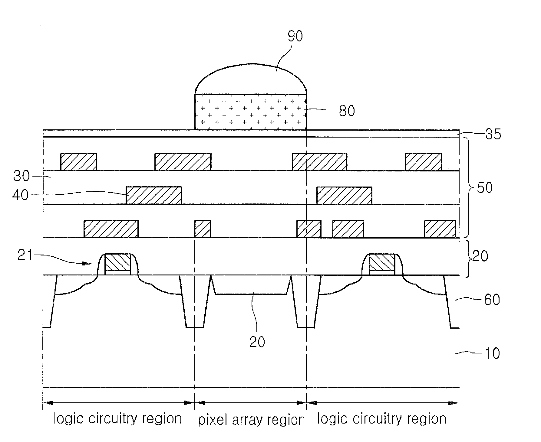
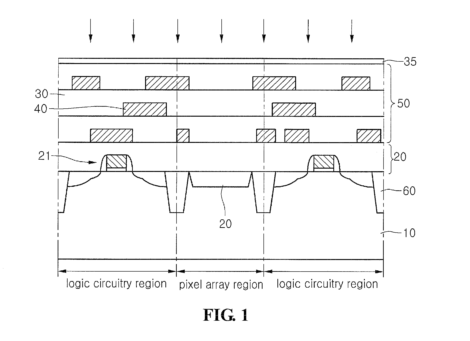
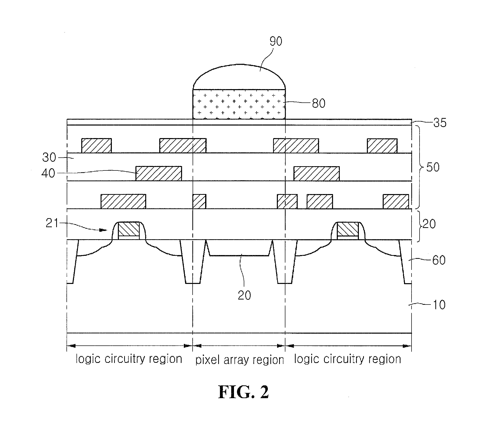
[0015]Hereinafter, methods of manufacturing a semiconductor device according to embodiments will be described in detail with reference to accompanying drawings. The size (dimension) of elements shown in the drawings may be magnified for the purpose of clear explanation and the real size of the elements may be different from the size of elements shown in drawings. In addition, the present invention may not include all the elements shown in the drawings and may not be limited thereto. The elements except for essential elements of the present invention can be omitted or added without limitation. In the description of embodiments, it will be understood that, when a layer (or film), a region, a pattern, or a structure is referred to as being “on (above / over / upper)” or “under (below / down / lower)” another substrate, another layer (or film), another region, another pad, or another pattern, it can be directly on the other substrate, layer (or film), region, pad or pattern, or intervening laye...


PUM


Abstract

Disclosed are methods of manufacturing a semiconductor device. The method of manufacturing one semiconductor device includes forming a transistor structure on a semiconductor substrate, forming a metal interconnection layer on the transistor structure, forming a protective layer on the metal interconnection layer, and implanting hydrogen ions into the semiconductor substrate having the protective layer by using a hydrogen ion implanter. Hydrogen ions are stably and effectively implanted into a selected region by using a hydrogen ion implanter in the manufacturing process of the semiconductor device, thereby facilitating the manufacturing process and improving the performance of the semiconductor device.

Description

CROSS-REFERENCE TO RELATED APPLICATION[0001]This application claims the benefit under 35 U.S.C. §119 of Korean Patent Application No. 10-2008-0119334, filed Nov. 28, 2008, which is hereby incorporated by reference in its entirety.BACKGROUND[0002]Generally, an image sensor is a semiconductor device that converts an optical image into an electric signal.[0003]Recently, the CMOS image sensor has been spotlighted as the next generation image sensor.[0004]A conventional CMOS image sensor includes a silicon substrate having a pixel region and a transistor region provided thereon with an interlayer dielectric layer including undoped silicon glass (USG), a bonding pad on the interlayer dielectric layer, and a protective layer on the interlayer dielectric layer having the bonding pad.[0005]The CMOS image sensor manufactured in such a manner has many dangling bonds on a gate insulating layer and the silicon substrate. The dangling bonds degrade the performance of the image sensor.[0006]In par...

Claims


Application Information

Patent Timeline
Patent Type & Authority Applications(United States)
IPC IPC(8): H01L21/26
CPCH01L27/14609H01L27/14621H01L27/14698H01L27/14685H01L27/14627H01L21/31H01L27/146
Inventor YANG, TAEK SEUNG
Owner DONGBU HITEK CO LTD
Why Eureka
Try Eureka