Method for processing the surface of an insulating article, printer head and substrate for recording medium

a technology of printing head and substrate, applied in the direction of magnetic materials for record carriers, instruments, record information storage, etc., can solve the problems of difficult to improve productivity, difficult to implant ions uniformly on the surface of articles, and prolonged process time, so as to improve hardness or tenacity, improve printing quality and operational reliability, and high-quality surface processing

Inactive Publication Date: 2006-11-28
SONY CORP
View PDF6 Cites 0 Cited by
  • Summary
  • Abstract
  • Description
  • Claims
  • Application Information

AI Technical Summary

Benefits of technology

[0011]It is therefore an object of the present invention to provide a surface processing method for an insulating material in which surface processing by ion implantation by the plasma implantation method can be realized effectively despite the fact that the article being processed is an insulating material. It is another object of the present invention to provide a printer head and a substrate for a recording medium each having on its surface a surface modified layer achieved as a result of ion implantation.
[0015]In the printer head of the present invention, in which the surface-modified layer is formed in its liquid droplet ejecting portion, it is possible to control the wettability to the ink of the liquid droplet ejecting portion and hence to prevent ink scorching or mixing of different sorts of inks in this liquid droplet ejecting portion.
[0017]The substrate for the recording medium according to the present invention is improved in hardness or tenacity by provision of the surface-modified layer on its surface.
[0018]In the surface processing method for the insulating material according to the present invention, there is no risk of electrical charges from being accumulated in the insulating material despite the fact that ion implantation is executed on the insulating material. Since the electrically conductive thin metal film is formed on the surface of the insulating material prior to ion implantation, the ions are implanted in a direction perpendicular to the surface of the insulating material, so that ions may be implanted effectively even if the insulating material has a three-dimensional surface profile. The result is that ion implantation can occur on end effectively even if ions are implanted in the insulating material. This assures high-quality surface processing for an insulating material.
[0019]In the printer head according to the present invention, in which a surface-modified layer is provided in the liquid droplet ejecting portion, it is possible to control the ink wettability in this liquid droplet ejecting portion. This prevents ink scorching or mixing of different sorts of inks in the liquid droplet ejecting portion to improve the printing quality and operational reliability.
[0020]In the substrate for a recording medium, according to the present invention, in which a surface-modified layer is provided on its surface, it is possible to improve hardness and tenacity. Thus, by employing the substrate for a recording medium according to the present invention, a recording medium of high reliability may be provided which is reduced in flexure or deviation from surface planarity to cope with the tendency towards high recording density.

Problems solved by technology

However, the ion beam implanting method suffers from the problem that, if an article being processed has a three-dimensional structure, it is difficult to implant ions uniformly on the article surface.
The result is that, if the plasma implantation method is applied to the insulating material, the process time is prolonged to render it difficult to improve the productivity.

Method used


Image

  • Method for processing the surface of an insulating article, printer head and substrate for recording medium
  • Method for processing the surface of an insulating article, printer head and substrate for recording medium
  • Method for processing the surface of an insulating article, printer head and substrate for recording medium

Examples


Embodiment Construction

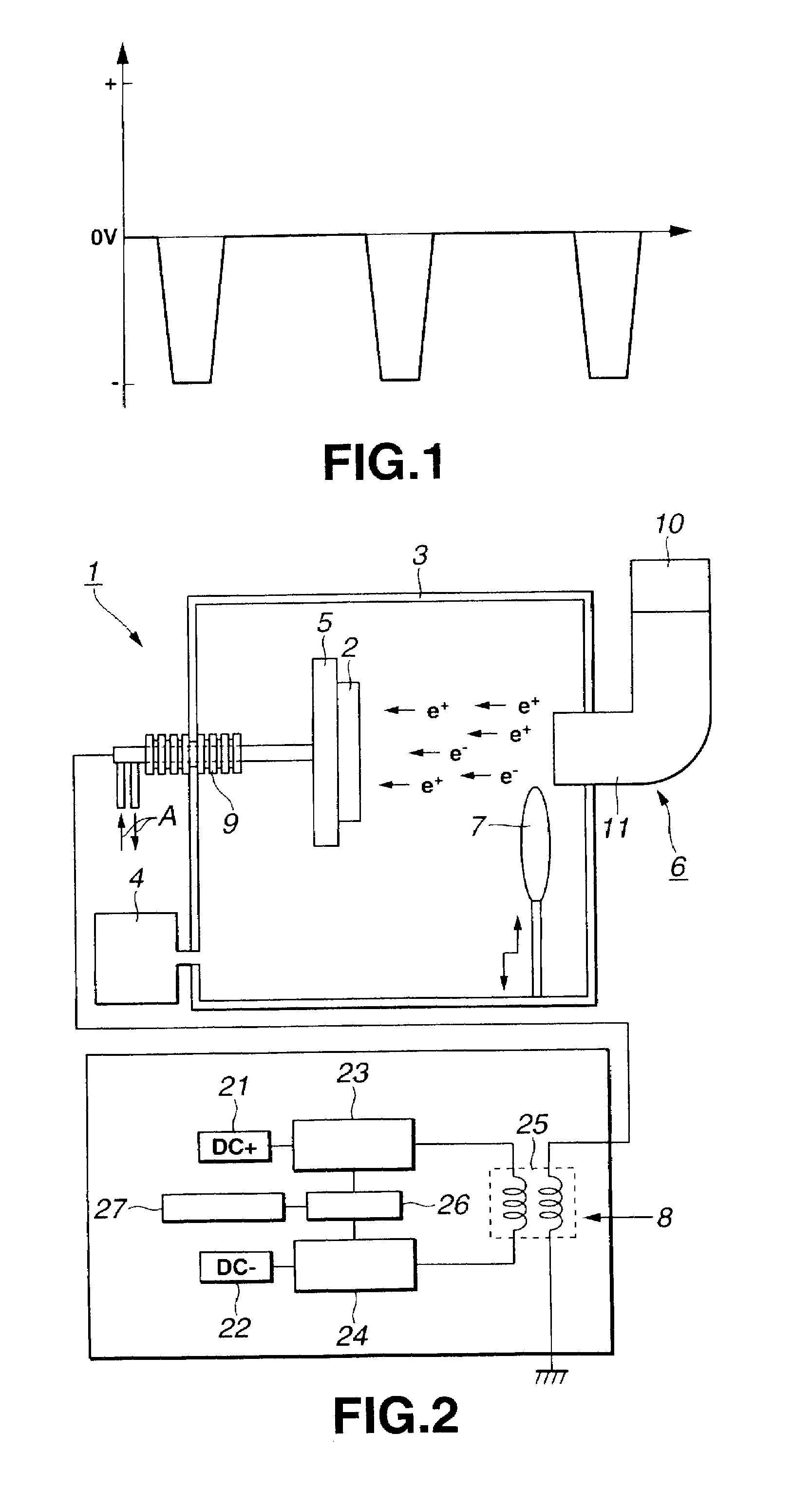
[0030]Referring to the drawings, preferred embodiments of according to the present invention will be explained in detail. As an illustrative structure of the surface processing device, used for surface processing an insulating material according to the present invention, a surface processing device 1, shown in FIG. 2, is explained. This surface processing device 1 processes the surface of a article 2 formed of an insulating material by implanting ions therein by the plasma implantation method.

[0031]The material of the article 2, to be surface-processed by the ion implantation, may be enumerated by, for example, plastic materials, such as amorphous polyolefin (APO), polycarbonate (PC), polymethyl methacrylate (PMMA), polyethylene terephthalate (PET), acrylic resin, polyimide resin, carbon materials and glass materials. The ion species implanted into the article may be enumerated by, for example, C, N, W, Ta, Cr, Mo, Co, Pt, Ni, Fe, Ti, Mn, Cu and Storage means.

[0032]This surface proc...


PUM

PropertyMeasurementUnit
pressureaaaaaaaaaa
pressureaaaaaaaaaa
thicknessaaaaaaaaaa

Abstract

A surface processing method for processing the surface of an insulating article in which an ion-implanted surface-modified layer is effectively formed on the article 2. In surface processing the article 2 of an insulating material, an electrically conductive thin metal film 50 is first formed on the article surface. A pulsed voltage containing a positive pulsed voltage and a negative pulsed voltage is applied to the article in a plasma containing ions to be implanted to implant ions in the article surface. This implants ions at right angles to the article surface to generate a surface-modified layer 51. There is no possibility of the article 2 being charged up due to application of a pulsed voltage.

Description

RELATED APPLICATION DATA[0001]This application claims priority to Japanese Patent Application No. P11-177193, filed Jun. 23, 1999, and is a divisional of U.S. patent application Ser. No. 09 / 598,308, filed Jun. 21, 2000 now U.S. Pat. No. 6,447,849BACKGROUND OF THE INVENTION[0002]1. Field of the Invention[0003]This invention relates to a surface processing method for processing the surface of an insulating article by ion injection and to a printer head provided in a printer configured for ejecting ink droplets to an article for printing to effect printing. This invention also relates to a substrate for a recording medium for supporting a signal recording layer of a recording medium.[0004]2. Description of Related Art[0005]For improving a variety of physical and chemical characteristics of an article being processed, such as hardness, elasto-plasticity, electrical conductivity, lubricating properties, durability, moisture-proofness, corrosion proofness, wettability or gas transmittance...

Claims


Application Information

Patent Timeline
Patent Type & Authority Patents(United States)
IPC IPC(8): G11B5/706G11B5/716B41J2/16C23C14/48G11B5/84G11B7/26H01J37/32
CPCC23C14/48H01J37/32412Y10T428/31678
Inventor WATANABE, SEIICHISHINOZAKI, KENJIKOHNO, MINORUMITSUHASHI, HIROYUKITONOSAKI, MINEHIROKOBAYASHI, MASATO
Owner SONY CORP
Why Eureka
Try Eureka