Systems and processes for forming three-dimensional circuits

a technology of three-dimensional circuits and processes, applied in the field of systems and processes for forming three-dimensional circuits, can solve the problems of increased complexity, increased manufacturing costs, and increased complexity, and achieves the effects of reducing complexity, improving manufacturing efficiency, and improving manufacturing efficiency

Inactive Publication Date: 2010-06-10
ULTRATECH INT INC
View PDF3 Cites 19 Cited by
  • Summary
  • Abstract
  • Description
  • Claims
  • Application Information

AI Technical Summary

Benefits of technology

[0017]For any of the embodiments of the invention, a controller may be used with a beam of radiation to effect heating. For example, when a radiation source and a stage is used, the radiation source may produce a beam for processing the second circuit layer, the stage may support and move the substrate relative to the beam, and the controller may provide relative scanning motion between the stage and the beam to allow the beam to scan over the second circuit layer. In addition, the radiation source may vary as well. For example, the radiation source may include a CO2 laser and / or a laser diode.

Problems solved by technology

While the benefits of faster devices with greater capability are clear, the cost for speed is correlated with increased complexity.
In turn, complexity is associated with higher manufacturing costs and lower manufacturing yields.
Until recently, cost metrics for the microelectronic device industry have continued to decrease primarily because manufacturing cost increases have risen slower than the physical size reductions for microelectronic devices.
However, as fundamental minimum feature sizes continue to shrink, the costs for achieving these smaller features are increasing exponentially.
At the 32 nm node, it is expected that the manufacturing costs will begin to rise faster than the reduction in transistor density.
In particular, the cost of new lithographic tools is a significant factor in the calculation of the cost metric for microelectronic devices.
In contrast, a state-of-the-art tool in 2008 cost nearly $50 million.
As a result, the integrated circuit industry appears to be approaching an unacceptable economic condition where the fundamental cost metric ($ / transistor) rises to a point that it may become unprofitable to produce devices with enhanced capability.
Consequently, cost reductions on traditional products (such as memory) may stagnate because further price reductions (through feature size shrinks) will be unachievable.
However, the dopants are implanted at interstitial sites, thereby increasing crystalline defect density in the substrate.
However, research into such three-dimensional circuits (3-D) has not been actively pursued for commercial devices because the increased costs associated with 3-D structures were higher than the costs of increasing density through lithography improvements.
Such attempts have not resulted in structures and device performance of commercial acceptability.
In particular, grain sizes associated with melted and recrystallized silicon are generally too small to ensure acceptable device performance.
Thus, there is a now an unfulfilled need for systems and processes for forming three-dimensional circuits on a substrate through laser annealing techniques and related technologies.

Method used


Image

  • Systems and processes for forming three-dimensional circuits
  • Systems and processes for forming three-dimensional circuits
  • Systems and processes for forming three-dimensional circuits

Examples


Embodiment Construction

Definitions and Overview

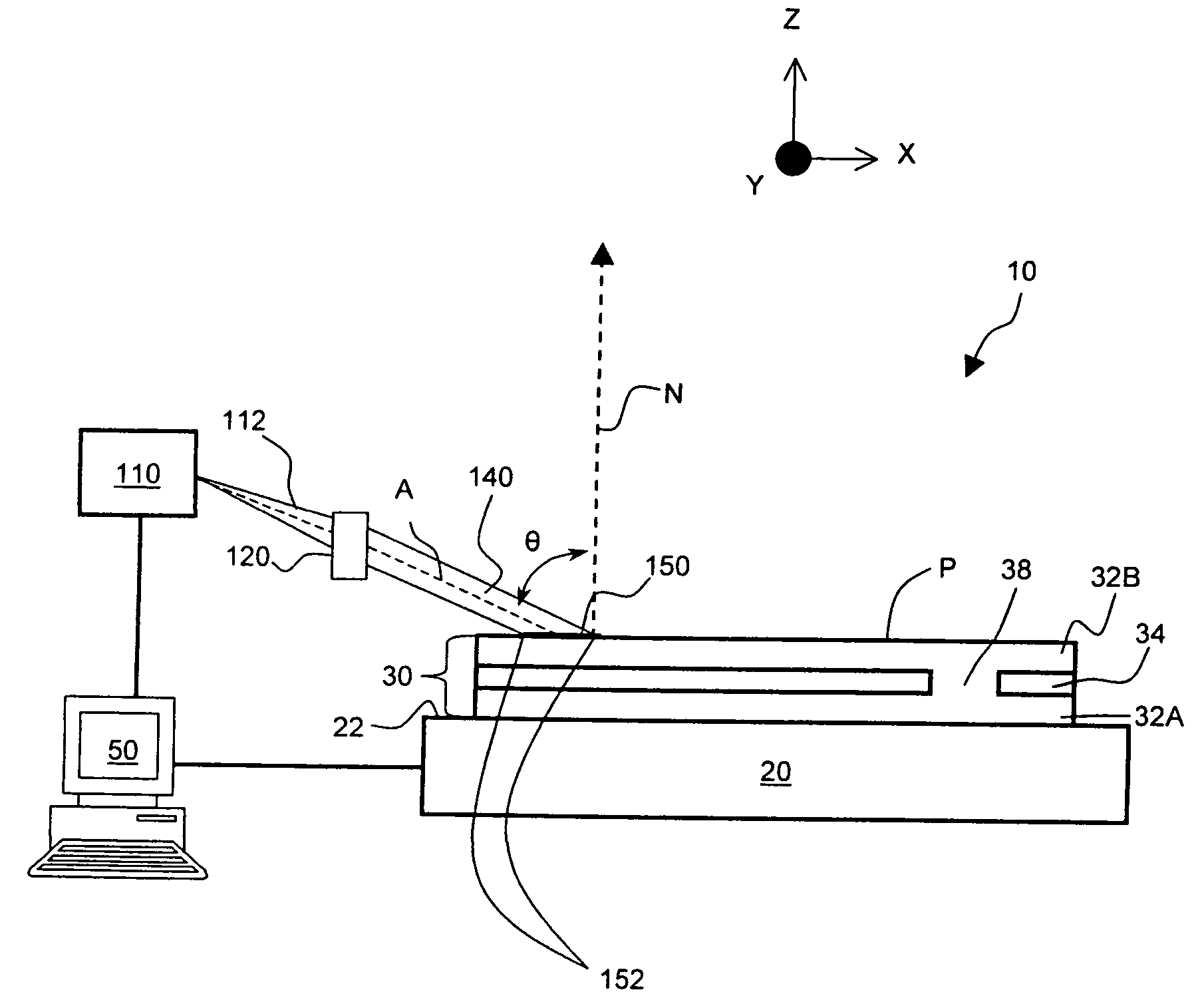
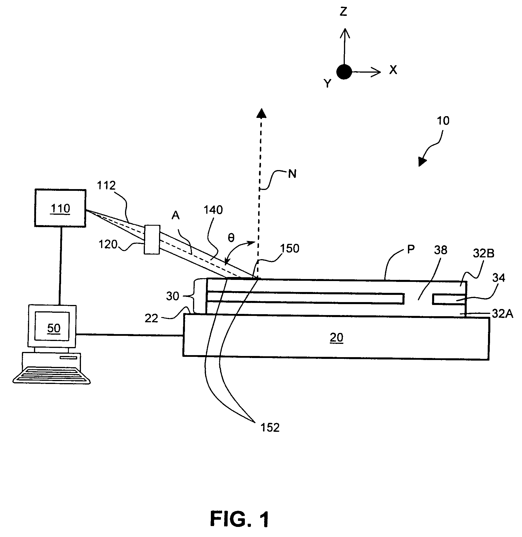
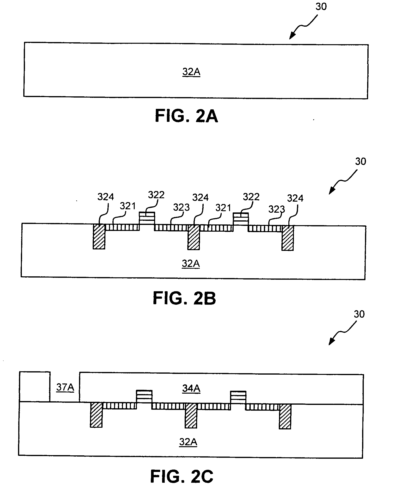
[0037]Before describing the present invention in detail, it is to be understood that this invention, unless otherwise noted, is not limited to specific substrates, lasers, or materials, all of which may vary. It is also to be understood that the terminology used herein is for the purpose of describing particular embodiments only, and is not intended to be limiting.

[0038]It must be noted that, as used in this specification and the appended claims, the singular forms “a”, “an” and “the” include both singular and plural referents unless the context clearly dictates otherwise. Thus, for example, reference to “a beam” includes a plurality of beams as well as a single beam, reference to “a circuit feature” includes a single circuit feature and a set of circuit features, “a layer” includes one or more layers, and the like.

[0039]In describing and claiming the present invention, the following terminology will be used in accordance with the following definitions.

[0040]...


PUM

PropertyMeasurementUnit
incidence angleaaaaaaaaaa
grain sizeaaaaaaaaaa
wavelengthaaaaaaaaaa

Abstract

Provided are systems and processes for forming a three-dimensional circuit on a substrate. A radiation source produces a beam that is directed at a substrate having an isolating layer interposed between circuit layers. The circuit layers communicate with reach other via a seed region exhibiting a crystalline surface. At least one circuit layer has an initial microstructure that exhibits electronic properties unsuitable for forming circuit features therein. After being controllably heat treated, the initial microstructure of the circuit layer having unsuitable properties is transformed into one that exhibits electronic properties suitable for forming circuit feature therein. Also provided are three-dimensional circuit structures optionally formed by the inventive systems and/or processes.

Description

BACKGROUND[0001]1. Field of the invention[0002]The invention relates generally to systems and processes for forming three-dimensional circuits, e.g., integrated circuits that include semiconductor circuit layers that communicate with each other. In particular, the invention relates such systems and processes that transform an initially unsuitable microstructure of a circuit layer into microstructure suitable for forming circuit features therein.[0003]2. Description of Background Art[0004]The performance of integrated circuits has continuously improved over time through increased speed and capability. This has primarily been achieved through the reduction of feature dimensions for microelectronic devices. Every few years, techniques have been developed to fabricate microelectronic devices with smaller dimensions, which generally produce faster integrated circuits in greater densities. In turn, devices comprised of greater quantities of faster intrinsic transistors may be produced, th...

Claims


Application Information

Patent Timeline
Patent Type & Authority Applications(United States)
IPC IPC(8): H01L23/58B23P19/00H01L21/00
CPCH01L21/8221Y10T29/53174Y10T117/1024H01L21/02532H01L21/02645H01L21/02678H01L27/0688
Inventor ZAFIROPOULO, ARTHUR W.WANG, YUNHAWRYLUK, ANDREW M.
Owner ULTRATECH INT INC
Why Eureka
Try Eureka