Method for manufacturing semiconductor device

a manufacturing method and semiconductor technology, applied in the direction of semiconductor devices, electrical devices, transistors, etc., can solve the problems of insufficient repair of fs layer b>9/b> defects, inability to achieve low-temperature (350° c. to 500° c.) heat treatment, and the effect of increasing the effect of heat on activation

Inactive Publication Date: 2012-12-27
FUJI ELECTRIC CO LTD
View PDF2 Cites 6 Cited by
  • Summary
  • Abstract
  • Description
  • Claims
  • Application Information

AI Technical Summary

Benefits of technology

[0048]When the substrate is heated during activation of the ion implantation layer, a state is assumed in which the ion implantation layer is easily activated under the effect of heating. In this case, when laser irradiation is performed, the effect of heat on activation is increased and activation is facilitated as opposed to the case of laser annealing performed at the room temperature. An especially significant effect of heating the substrate is produced on layers that are deep from the laser irradiation face because the heat of laser radiation is unlikely to penetrate thereto. Such an approach is effective for activating the FS layer. Further, crystal defects in the ion implantation layer can be sufficiently repaired. In addition, since the temperature of the front face structure is maintained less than or equal to 500° C. during laser annealing, no adverse effects (oxidation, melting, etc.) are produced on the emitter electrode. As a result, it is possible to provide a method for manufacturing a semiconductor device with good characteristics and a high activation ratio.
[0049]An effect demonstrated by the semiconductor apparatus in accordance with embodiments of the present invention is that the activation ratio of the dopant that has been ion implanted in the back face can be increased without adversely affecting the front face structure of the device. Additionally, since the crystal defects caused by ion implantation can be sufficiently repaired, another effect is that the desired diffusion profile can be obtained with a small spread.

Problems solved by technology

With the development of next-generation insulated gate bipolar transistors, transistors with novel chip structures and lower ON voltage have been developed, which has resulted in a decrease in loss and increase in efficiency of application equipment.
First, when the activation ratio is increased so as to obtain a predetermined diffusion profile in the FS layer 9 of a FS-type IGBT, this cannot be attained by low-temperature (350° C. to 500° C.) heat treatment in an electric furnace.
Second, when the FZ-N substrate 1 is in a room temperature state, the repair of defects in the FS layer 9 is insufficient when a laser annealing method has been used.
Third, in the usual laser annealing apparatus, no mechanism is provided for heating the substrate.
Fifth, a problem associated with the method described in Patent Document 1 is that when ion implantation and laser annealing are performed simultaneously while heating the substrate, regions appear in the substrate, into which ions have been implanted but have not yet been irradiated with laser light, unless control is performed to ensure the duration of ion implantation is substantially similar to the duration of laser irradiation.
As a result, the size of the manufacturing apparatus is very large.
Further, when dopants with a low penetration depth and dopants with a high penetration depth in ion implantation are activated at the same time, the dopants of both types are difficult to activate with good efficiency.
Where the irradiation energy density is outside the above-mentioned range, a high activation ratio is difficult to obtain or an adverse effect is produced on the front face structure.

Method used


Image

  • Method for manufacturing semiconductor device
  • Method for manufacturing semiconductor device
  • Method for manufacturing semiconductor device

Examples


embodiment 1

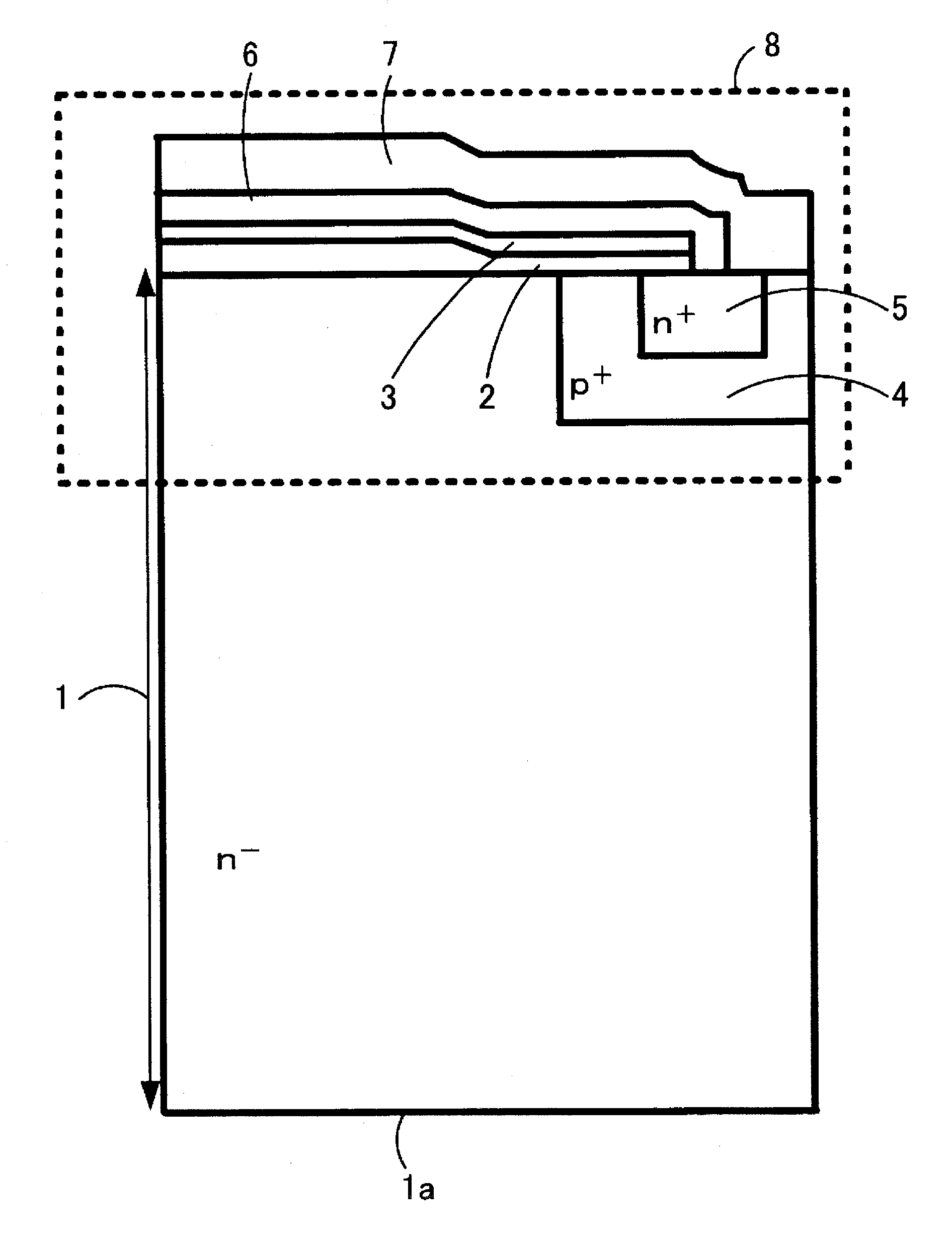
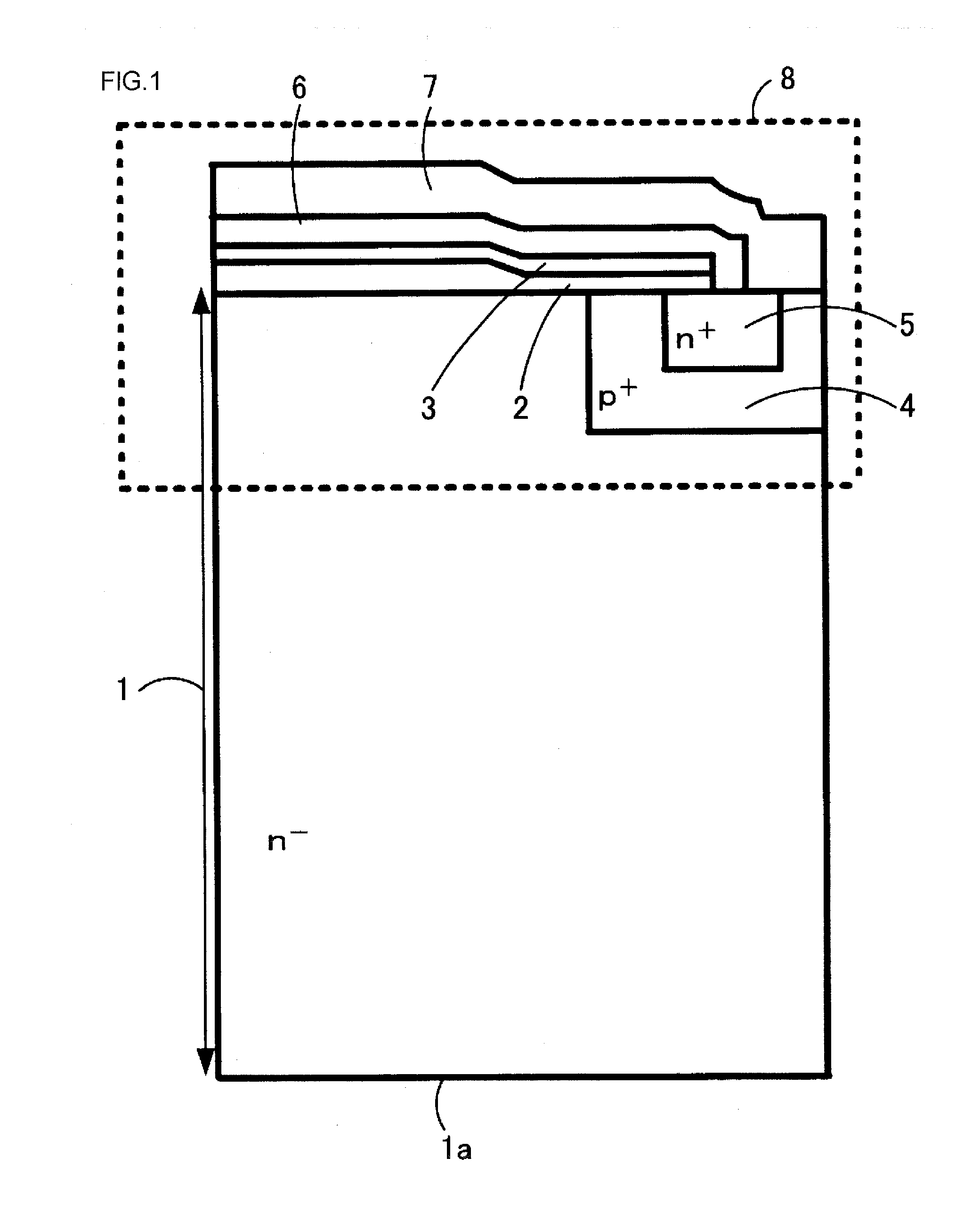
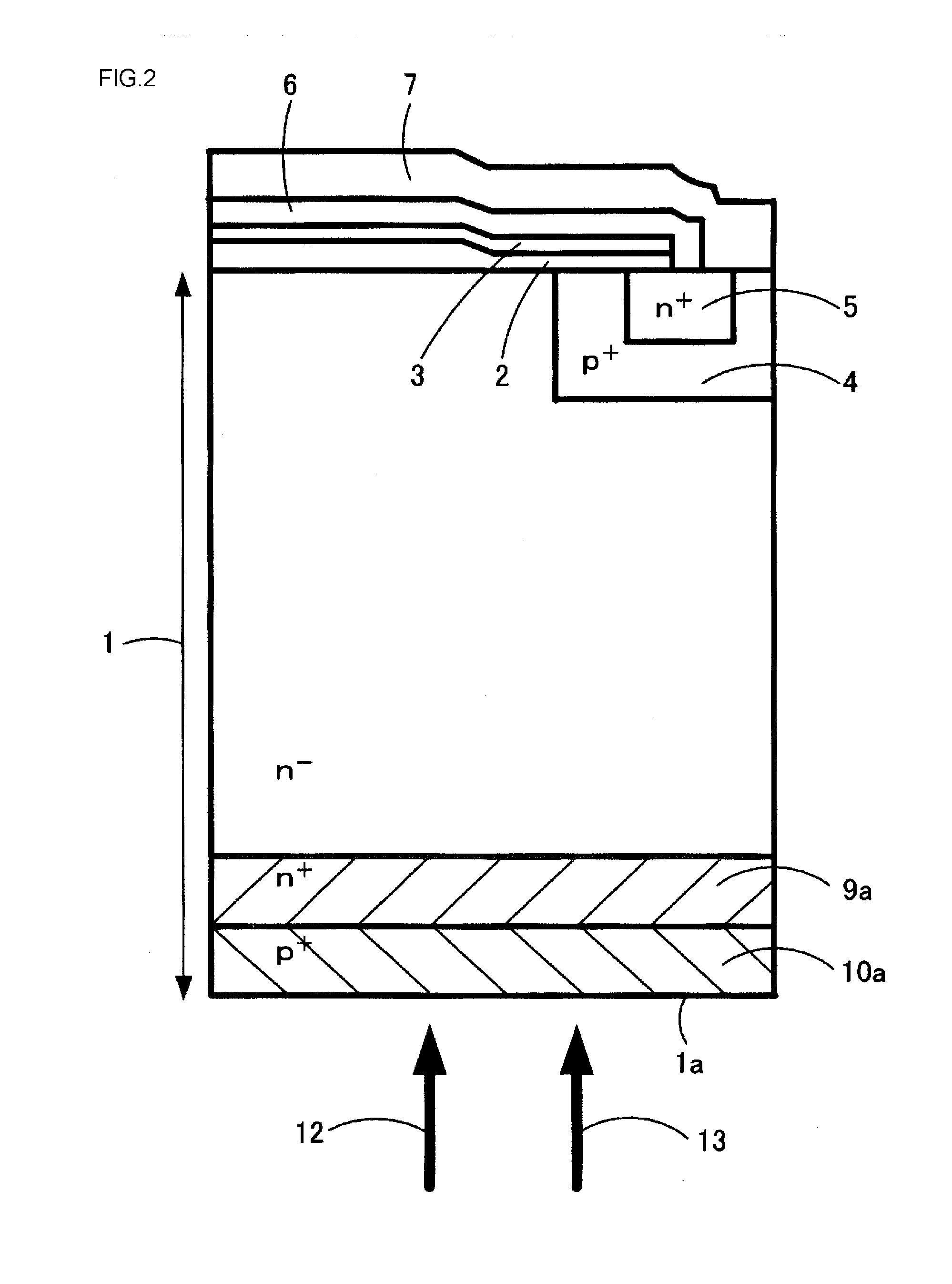
[0072]FIGS. 1 to 4 are cross-sectional views illustrating the method for manufacturing a semiconductor device according to Embodiment 1. In FIGS. 1 to 4, the cross-sectional views of the principal portion of the semiconductor device in the manufacturing process are shown in sequence. A FS-type IGBT 100 (see FIG. 4) is considered as an example of the semiconductor device. In the manufacturing process, the process performed on the front face side is identical to the conventional process (see FIGS. 12 to 14). Therefore, only the back face side process is explained herein. Portions identical to those of the conventional configuration are assigned with same reference numerals.

[0073]A front face structure 8 is formed on the front face of a FZ-N substrate 1b. Then, as shown in FIG. 14, the FZ-N substrate 1b is polished by back grinding or etching to the desired thickness from the back face side of the FZ-N substrate 1b and a thin wafer is obtained. As a result, a thin-film FZ-N substrate 1...

example

[0077]The preferred conditions of ion implantation and laser annealing will be explained below. FIG. 5 is a characteristic diagram illustrating the diffusion profile of the FS-type IGBT 100. The diffusion profile is a concentration profile measured by a Spreading Resistance (SR) method. In accordance with Embodiment 1, two types of FS-type IGBT 100 were fabricated that had different substrate temperatures during the fabrication process. The substrate temperatures were (a) room temperature (no heating; dot line in FIG. 5) and (b) 300° C. (the substrate was heated; solid line in FIG. 5). After the substrate temperature has reached the predetermined temperature, the substrate was held for 5 min and then laser annealing was performed by irradiating the back face of the substrate with laser light. A YAG 2ω laser was used as the laser, the irradiation energy density of the laser light was 4 J / cm2, and the pulse width was 100 ns.

[0078]The ion implantation conditions were as follows: ion im...

embodiment 2

[0101]FIG. 8 is a configuration diagram illustrating the principal portion of the apparatus for manufacturing a semiconductor device according to Embodiment 2. In the manufacturing apparatus shown in FIG. 8, laser annealing is performed to activate the ion-implanted dopants. This manufacturing apparatus is constituted by the laser irradiation unit 15, the optical system mirror 16 guiding the laser light 14 to the FZ-N substrate 1 (wafer), the substrate heating unit 31 that heats the FZ-N substrate 1, and a guide 32 (claw) fixing the FZ-N substrate 1 to the substrate heating unit 31. For example, the manufacturing apparatus shown in FIG. 8 can be used for manufacturing the semiconductor device according to Embodiment 1. By arranging the guide 32 that fixes the FZ-N substrate 1 to the substrate heating unit 31, it is possible to realize both a support unit for supporting the FZ-N substrate 1 and a heating unit for heating the FZ-N substrate 1.

[0102]With the manufacturing apparatus sho...


PUM


Abstract

A method for manufacturing a semiconductor device, the method including forming a front face structure of a semiconductor device on a first main face of a semiconductor substrate, grinding a second main face of the semiconductor substrate and reducing the semiconductor substrate in thickness to a thickness equal to or less than 100 μm, ion implanting a dopant into the second main face of the semiconductor substrate of reduced thickness, and activating the dopant by irradiating the second main face with laser light and performing laser annealing while the semiconductor substrate of reduced thickness is heated.

Description

CROSS-REFERENCE TO RELATED APPLICATIONS[0001]This application is a continuation, under 35 U.S.C. 111(a), of international application No. PCT / JP2011 / 051625 filed on Jan. 27, 2011, which claims priority to Japanese Patent Application No. 2010-023378, filed on Feb. 4, 2010, the disclosures of which are incorporated herein by reference.BACKGROUND[0002]1. Field[0003]The present invention relates to a method for manufacturing a semiconductor device.[0004]2. Description of the Related Art[0005]Power integrated circuits (IC), in which electric circuits are comprised of a large number of transistors or resistors and integrated power semiconductor devices, have been widely used for important components of computers and communication equipment.[0006]An insulated gate bipolar transistor (IGBT) is a power semiconductor device which combines high-speed switching and voltage drive characteristics of a MOSFET (MOS gate field-effect transistor) with low ON voltage characteristic of a bipolar transi...

Claims


Application Information

Patent Timeline
Patent Type & Authority Applications(United States)
IPC IPC(8): H01L21/265
CPCH01L29/66333H01L21/268H01L29/42368H01L29/7395
Inventor NAKAZAWA, HARUO
Owner FUJI ELECTRIC CO LTD
Why Eureka
Try Eureka