
Branched waveguide multisection dbr semiconductor laser

a semiconductor laser and waveguide technology, applied in the direction of semiconductor lasers, optical resonators, optical elements, etc., can solve the problems of large size and expensive installation, significant redundancy, and not desirable within the size limited optical telecommunications packag

Active Publication Date: 2010-06-10
LUMENTUM TECH UK LTD
View PDF14 Cites 58 Cited by
  • Summary
  • Abstract
  • Description
  • Claims
  • Application Information

AI Technical Summary

Benefits of technology

The present invention provides a tunable semiconductor laser with a branched optical waveguide that has a stem optical reflector and at least two branch waveguides. The laser emits light at a wavelength within a first wavelength range and can be tuned within a second wavelength range. The laser can be operated with a single tunable branch optical reflector or with a combination of tunable branch optical reflectors. The laser can provide wavelength tuning over a greater range than a laser with just one tunable branch optical reflector. The laser can also have a gain section and phase control sections for very fine tuning of the lasing wavelength. The laser can be used in a variety of applications such as optical communication systems and optical sensors.

Problems solved by technology

Historically it has been common to use separate devices to operate at each channel, which has required a discrete device to be installed in a network for each possible channel, making the installation large in size and expensive, whilst also commonly resulting in a significant level of redundancy, since typically not all available channels will be used.
Disadvantageously, for a wide range of operating channels, monolithically integrated arrays of independent DBR lasers require large laser chips, which are not desirable within size limited optical telecommunications packages.
Further, the complexity of such chips will typically reduce the possible manufacturing yield, and the complexity of electrical control required to operate the chip may significantly increase the cost of the associated control system.
This condition provides a fundamental limitation upon the breadth of tuning range that is achievable with the Vernier tuning method.
However, increasing the wavelength range of the second DBR 304 necessitates that it should be longer, thus increasing the length of the lasing cavity, and the closeness of the optical modes within the cavity with respect to wavelength, which may increase the strength of unwanted optical side modes to the lasing mode.

Method used


Image

  • Branched waveguide multisection dbr semiconductor laser
  • Branched waveguide multisection dbr semiconductor laser
  • Branched waveguide multisection dbr semiconductor laser

Examples


Embodiment Construction

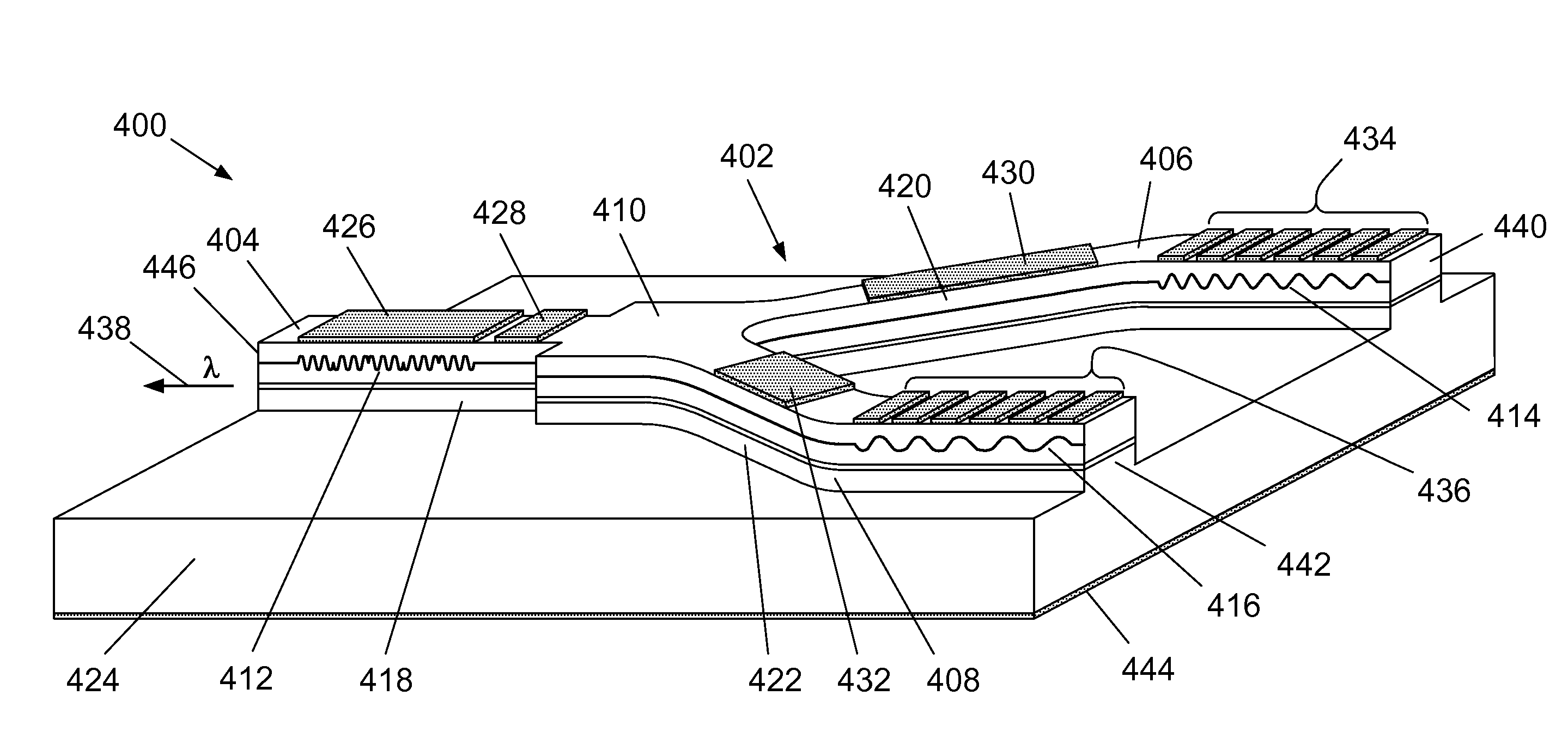
[0045]FIG. 4 shows schematically a first embodiment of the present invention. A semiconductor laser 400 has a Y-shaped, branched optical waveguide 402. The illustrated optical waveguide is a ridge waveguide, although other designs of waveguide may also be suitable and will be known to those skilled in the art. The optical waveguide 402 comprises a “stem” waveguide section 404, a first “branch” waveguide section 406 and a second “branch” waveguide section 408. The first and second branch waveguide sections 406 and 408 are optically in parallel, and optically coupled to the stem waveguide section 404 by means of a 1×2 optical coupler 410. A stem optical reflector 412 is provided in the stem waveguide section 404, and is tunable. First and second tunable branch optical reflectors 414, 416 are respectively disposed on the first branch and second branch waveguide sections 404, 406 and 408.

[0046]The optical reflectors 412, 414, 416 are distributed Bragg reflectors (DBRs), comprising grati...


PUM


Abstract

The present invention concerns tunable distributed Bragg reflector (DBR) semiconductor lasers, in particular a DBR laser with a branched optical waveguide 5 within which a plurality of differently shaped lasing cavities may be formed, and a method of operation of such a laser. The laser may comprise a phase control section (418), gain section (420, 422), a sampled grating DBR (412) giving a comb-line spectrum and two tunable, chirped DBRs (414, 416) for broadband frequency training and a coupling section (410).

Description

TECHNICAL FIELD OF THE INVENTION[0001]The present invention concerns distributed Bragg reflector (DBR) semiconductor lasers, in particular a DBR laser with a branched optical waveguide.BACKGROUND OF THE INVENTION[0002]In the field of optical telecommunications lasers are used to generate optically encoded signals that are transmitted along optical fibres, typically at wavelengths corresponding to channels of the International Telecommunications Union (ITU) grid. The lasers commonly used are monolithically integrated semiconductor lasers.[0003]Different types of semiconductor lasers are commercially available. Distributed feedback (DFB) and distributed Bragg reflector (DBR) lasers with very narrow tuning ranges may be used to provide single channel operation at a substantially fixed wavelength. Historically it has been common to use separate devices to operate at each channel, which has required a discrete device to be installed in a network for each possible channel, making the inst...

Claims


Application Information

Patent Timeline
Patent Type & Authority Applications(United States)
IPC IPC(8): H01S3/1055H01S3/10H01S5/125H01S5/00
CPCG02B2006/12107H01S5/026H01S5/06256H01S5/10H01S5/1003H01S5/4087H01S5/1209H01S5/1212H01S5/141H01S5/4062H01S5/4068H01S5/1092
Inventor WARD, ANDREWWALKER, ROBERTROBBINS, DAVID JAMESREID, DOUGLASTOWLSON, GUY
Owner LUMENTUM TECH UK LTD
Learn More