Semiconductor device and method of manufacturing the same

a semiconductor device and manufacturing method technology, applied in the direction of semiconductor devices, semiconductor/solid-state device details, electrical apparatus, etc., can solve the problems of difficult to apply this manufacturing method to a semiconductor device that requires high-speed operation, difficult to obtain a semiconductor device suitable for high-speed operation, and a possible problem of interconnect length of 2 to 3 mm, so as to reduce the path length of signals transmitted, prevent metal contamination, and reduce the effect of path length

Active Publication Date: 2010-06-10
RENESAS ELECTRONICS CORP
View PDF12 Cites 21 Cited by
  • Summary
  • Abstract
  • Description
  • Claims
  • Application Information

AI Technical Summary

Benefits of technology

[0018]In this manufacturing method, electrical connection between the first semiconductor chip and another semiconductor chip is established by the through electrode. This reduces the path length of the signals transmitted between the two chips as compared with the case in which the electrical connection between these two chips is established by an interconnect that detours through the outside of the chips. For this reason, a semiconductor device suitable for high-speed operation can be obtained.
[0019]Further, an inorganic insulating layer is formed that directly covers the back surface of the first semiconductor chip. This inorganic insulating layer prevents the device region (the region where semiconductor elements such as transistors are to be formed) of the semiconductor chip from being contaminated with metals. For this reason, the problem of metal contamination can be prevented from occurring even if the semiconductor chip is thinned, unlike the case in which the back surface of the semiconductor chip is stripped bare.
[0022]In this semiconductor device, electrical connection between the first semiconductor chip and another semiconductor chip is established by the through electrode. This reduces the path length of the signals transmitted between the two chips as compared with the case in which the electrical connection between these two chips is established by an interconnect that detours through the outside of the chips. For this reason, a semiconductor device suitable for high-speed operation can be realized.
[0023]Further, an inorganic insulating layer is provided that directly covers the back surface of the first semiconductor chip. This inorganic insulating layer prevents the device region of the semiconductor chip from being contaminated with metals. For this reason, the problem of metal contamination can be prevented from occurring even if the semiconductor chip is thinned, unlike the case in which the back surface of the semiconductor chip is stripped bare.

Problems solved by technology

However, according to the manufacturing methods disclosed in the patent documents 1, 2, it is difficult to obtain a semiconductor device suitable for high-speed operation.
When the interconnect length is large, there will be a delay in the signals, so that it is difficult to apply this manufacturing method to a semiconductor device that requires a high-speed operation.
For example, when considering the connection to a DDR2 (Double Data Rate 2) memory, even an interconnect length of about 2 to 3 mm could be a problem.
Moreover, the manufacturing methods disclosed in the patent documents 1-4 are all unsuitable for manufacturing a semiconductor device on which a thin type semiconductor chip is mounted.
The reason lies in that, with regard to the patent document 1, since the back surface of the semiconductor chip is stripped bare, a problem of metal contamination will occur when the thickness of the chip is reduced.
Such metal contamination will give adverse effects on the semiconductor device.
When the chip is extremely thin (for example, less than 50 μm), the chip will be damaged even with a little force, so that it is difficult to handle a single chip.
Also, due to the stress between the silicon and the insulating layer, the chip will be greatly warped when a free surface is given to the chip, thereby making the handling all the more difficult.

Method used


Image

  • Semiconductor device and method of manufacturing the same
  • Semiconductor device and method of manufacturing the same
  • Semiconductor device and method of manufacturing the same

Examples


Embodiment Construction

[0049]The invention will be now described herein with reference to illustrative embodiments. Those skilled in the art will recognize that many alternative embodiments can be accomplished using the teachings of the present invention and that the invention is not limited to the embodiments illustrated for explanatory purposes.

[0050]Hereafter, preferable embodiments of a semiconductor device and a method of manufacturing the same according to the present invention will be described in detail with reference to the attached drawings. Here, in the description of the drawings, the same elements will be denoted with the same reference numerals, and the description thereof will not be repeated.

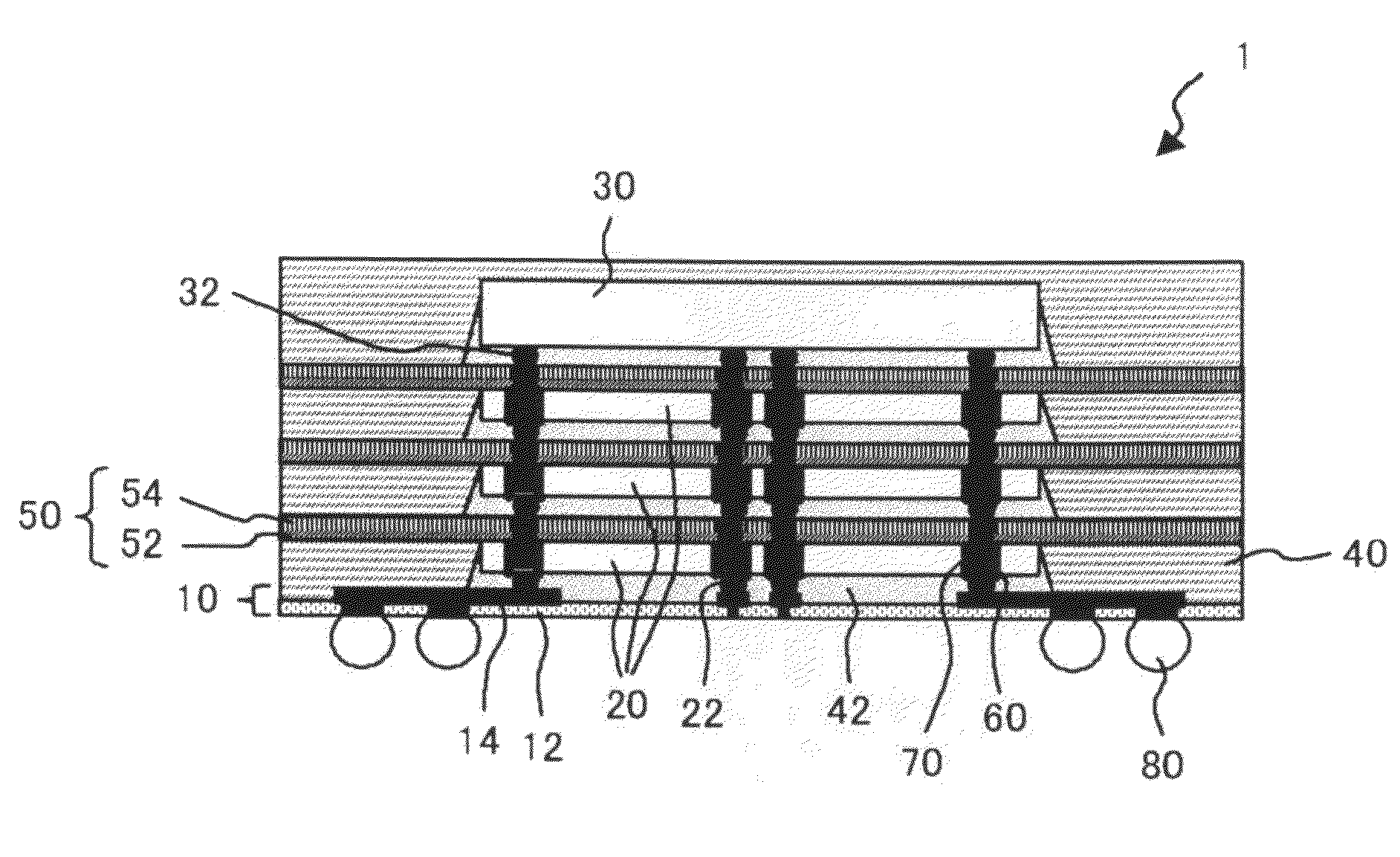
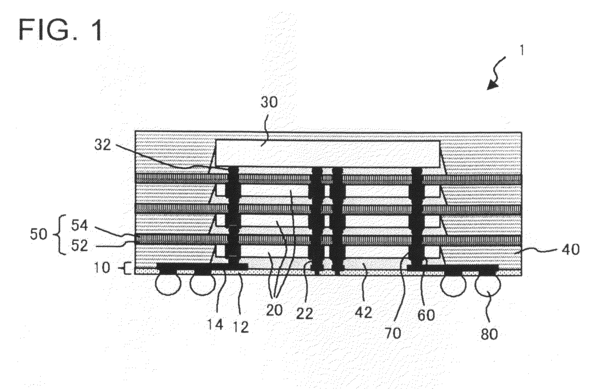
[0051]FIG. 1 is a cross-sectional view illustrating an embodiment of a semiconductor device according to the present invention. The semiconductor device 1 includes an interconnect member 10, a semiconductor chip 20 (first semiconductor chip), a semiconductor chip 30 (second semiconductor chip), a resin...


PUM


Abstract

A method of manufacturing a semiconductor device includes forming an interconnect member, mounting a first semiconductor chip having a semiconductor substrate in a face-down manner on the interconnect member, forming a resin layer on the interconnect member to cover a side surface of the first semiconductor chip, thinning the first semiconductor chip and the resin layer, forming an inorganic insulating layer on a back surface of the first semiconductor chip so as to be in contact with the back surface and to extend over the resin layer, and forming a through electrode so as to penetrate the inorganic insulating layer and the semiconductor substrate.

Description

[0001]The present application is a Divisional Application of U.S. patent application Ser. No. 11 / 602,346, filed on Nov. 21, 2006, which is based on Japanese patent application No. 2005-349794, incorporated herein by reference.BACKGROUND[0002]1. Technical Field[0003]The present invention relates to a semiconductor device and a method of manufacturing the same.[0004]2. Related Art[0005]As a conventional method of manufacturing a semiconductor device, there is a method disclosed in Japanese Laid-Open patent publication No. 2002-343904 (patent document 1), for example. This document discloses a method of manufacturing a multiple-chip type semiconductor device in which a plurality of semiconductor chips are stacked.[0006]According to the manufacturing method disclosed in the patent document 1, first, a printed substrate is prepared in which an electrode post is formed on one surface, and a connection electrode is formed on the other surface. Next, a semiconductor chip is mounted in a fac...

Claims


Application Information

Patent Timeline
Patent Type & Authority Applications(United States)
IPC IPC(8): H01L21/50
CPCH01L21/76898H01L23/3128H01L2924/10155H01L2224/73204H01L2224/32225H01L2224/16225H01L2924/15311H01L2924/01079H01L2924/01078H01L2924/01046H01L23/481H01L23/562H01L23/642H01L25/0657H01L25/50H01L2221/68345H01L2223/6622H01L2224/16145H01L2225/06513H01L2225/06517H01L2225/06524H01L2225/06541H01L2225/06572H01L2924/00H01L2924/181H01L2224/73259H01L2224/81005H01L2224/83005H01L2224/12105H01L2224/04105H01L2224/13025H01L2924/3511H01L2924/00012
Inventor KAWANO, MASAYASOEJIMA, KOJITAKAHASHI, NOBUAKIKURITA, YOICHIROKOMURO, MASAHIROMATSUI, SATOSHI
Owner RENESAS ELECTRONICS CORP
Why Eureka
Try Eureka