Germanium FinFETs Having Dielectric Punch-Through Stoppers

Active Publication Date: 2010-06-10
TAIWAN SEMICON MFG CO LTD
View PDF53 Cites 249 Cited by
  • Summary
  • Abstract
  • Description
  • Claims
  • Application Information

AI Technical Summary

Benefits of technology

[0014]The advantageous features of the present invention include reduced punch-through currents

Problems solved by technology

The oxide of germanium, on the other hand, is soluble in water, and hence is not suitable for the formation of gate dielectrics.
A challenge faced by the semiconductor industry is that to reduce the leakage of MOS transistors and to increase the drive currents of germanium FinFETs, germanium-on-insulator (GOI) structures need to be formed.
However, the price of GOI substrates (and strained GOI (SGOI) substrates) is many

Method used


Image

  • Germanium FinFETs Having Dielectric Punch-Through Stoppers
  • Germanium FinFETs Having Dielectric Punch-Through Stoppers
  • Germanium FinFETs Having Dielectric Punch-Through Stoppers

Examples


Embodiment Construction

[0019]The making and using of the presently preferred embodiments are discussed in detail below. It should be appreciated, however, that the present invention provides many applicable inventive concepts that can be embodied in a wide variety of specific contexts. The specific embodiments discussed are merely illustrative of specific ways to make and use the invention, and do not limit the scope of the invention.

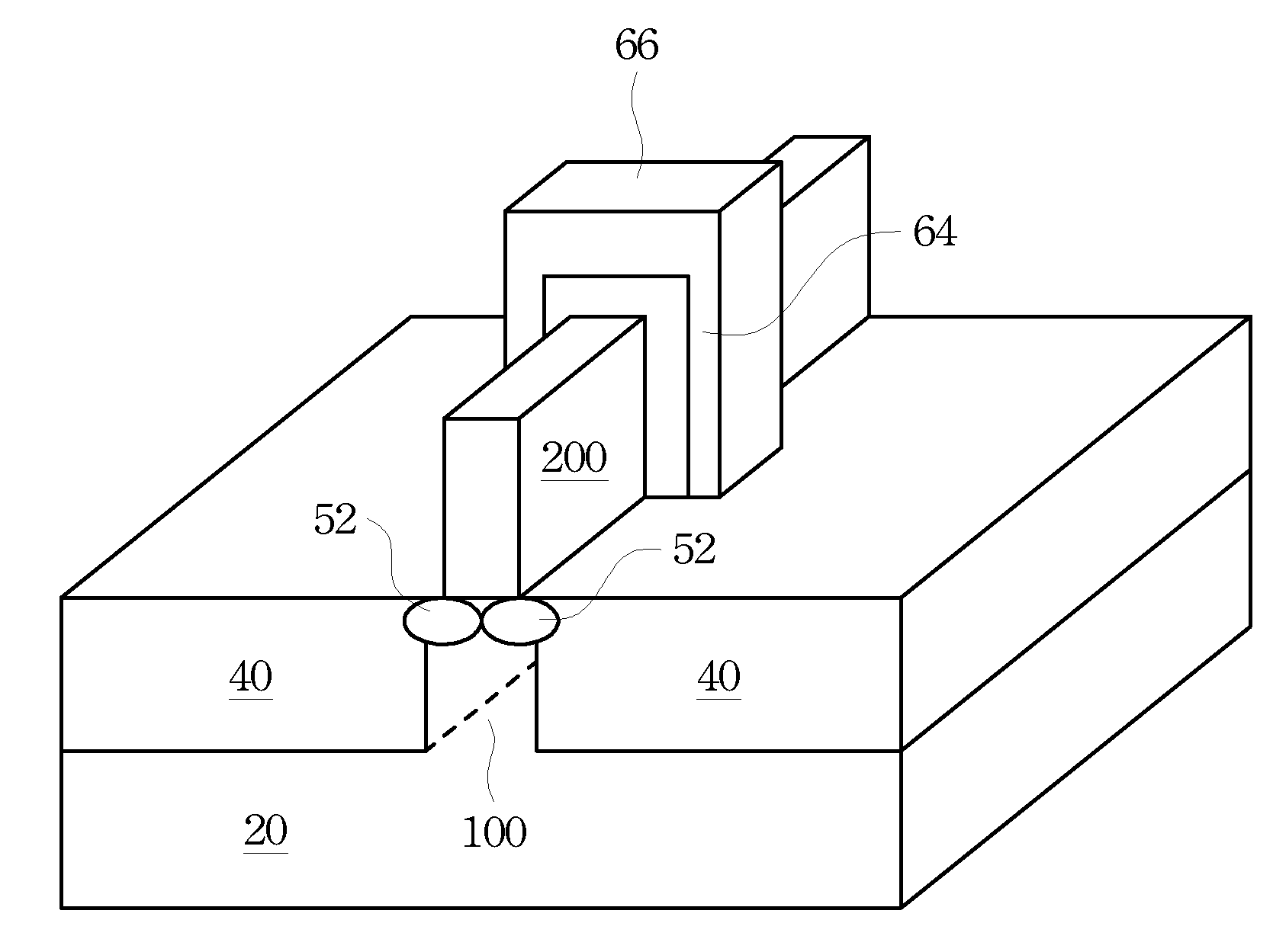
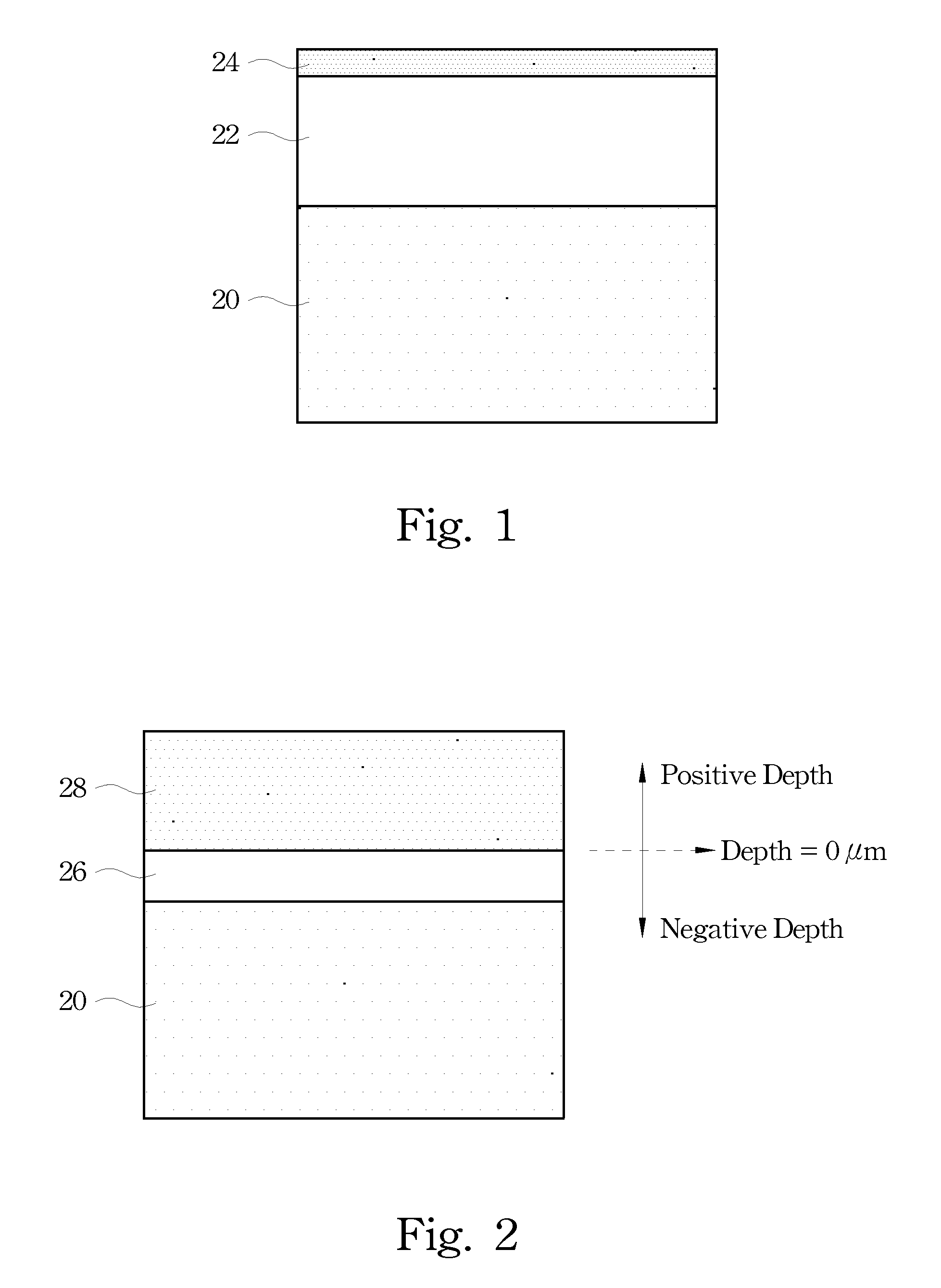
[0020]An integrated circuit formation process including the formation of a germanium fin that may be used to form a fin field-effect transistor (FinFET, also referred to as a multi-gate transistor) is provided. The intermediate stages of manufacturing a preferred embodiment of the present invention are illustrated. The variations of the preferred embodiments are discussed. Throughout the various views and illustrative embodiments of the present invention, like reference numbers are used to designate like elements.

[0021]Embodiments of the invention relate to semiconductor stru...


PUM


Abstract

A method of forming a semiconductor structure includes providing a composite substrate, which includes a bulk silicon substrate and a silicon germanium (SiGe) layer over and adjoining the bulk silicon substrate. A first condensation is performed to the SiGe layer to form a condensed SiGe layer, so that the condensed SiGe layer has a substantially uniform germanium concentration. The condensed SiGe layer and a top portion of the bulk silicon substrate are etched to form a composite fin including a silicon fin and a condensed SiGe fin over the silicon fine. The method further includes oxidizing a portion of the silicon fin; and performing a second condensation to the condensed SiGe fin.

Description

CROSS-REFERENCE TO RELATED APPLICATION[0001]This application relates to commonly assigned U.S. patent application Ser. No. 12 / 116,074, filed May 6, 2008, and entitled “FinFETs Having Dielectric Punch-Through Stoppers,” which application is incorporated herein by reference.TECHNICAL FIELD[0002]This invention relates generally to semiconductor devices, and particularly to structures and formation methods of germanium nano-wires and Fin field-effect transistors (FinFETs) having germanium fins.BACKGROUND[0003]Germanium is a commonly known semiconductor material. The electron mobility and hole mobility of germanium are greater than that of silicon, hence making germanium an excellent material in the formation of integrated circuits. However, in the past, silicon gained more popularity since its oxide (silicon oxide) is readily usable in the gate dielectric of metal-oxide-semiconductor (MOS) transistors. The gate dielectrics of the MOS transistors can be conveniently formed by thermal oxi...

Claims


Application Information

Patent Timeline
IPC IPC(8): H01L21/20H01L21/28
CPCH01L21/02381H01L21/0245H01L21/02532H01L29/7851H01L29/1054H01L29/66795H01L21/02617
Inventor CHANG, CHENG-HUNGHSU, YU-RUNGLEE, CHEN-YIHUNG, SHIH-TINGYEH, CHEN-NANYU, CHEN-HUA
Owner TAIWAN SEMICON MFG CO LTD
Why Eureka
Try Eureka