Integrated structure of MEMS device and CMOS image sensor device and fabricating method thereof

a technology of integrated structure and cmos image sensor, which is applied in the field of integrated structure of microelectromechanical systems, can solve the problems of not being able to integrate mems microphone and cis device, cfa and the microlens on the front side of the silicon substrate are unavoidably damaged during the fabrication of vent holes, etc., and achieve the effect of not increasing process complexity and cos

Active Publication Date: 2010-06-17
UNITED MICROELECTRONICS CORP
View PDF2 Cites 15 Cited by
  • Summary
  • Abstract
  • Description
  • Claims
  • Application Information

AI Technical Summary

Benefits of technology

[0013]According to the integrated structure of MEMS device and CIS device and fabricating method provided by the present invention, the CFA and the microlens array are both formed on the back side of the substrate; therefore the CFA and the microlens array are prevented from being damaged during forming the vent holes on the back side of the substrate. More noteworthy, since the material used to form the mask p

Problems solved by technology

However, when integrating the MEMS microphone and the CIS device, a problem emerges: The CFA of the CIS device is formed on the front side of the silicon substrate while fabrication of the vent holes of the MEMS microphone is performed on the back

Method used


Image

  • Integrated structure of MEMS device and CMOS image sensor device and fabricating method thereof
  • Integrated structure of MEMS device and CMOS image sensor device and fabricating method thereof
  • Integrated structure of MEMS device and CMOS image sensor device and fabricating method thereof

Examples


Embodiment Construction

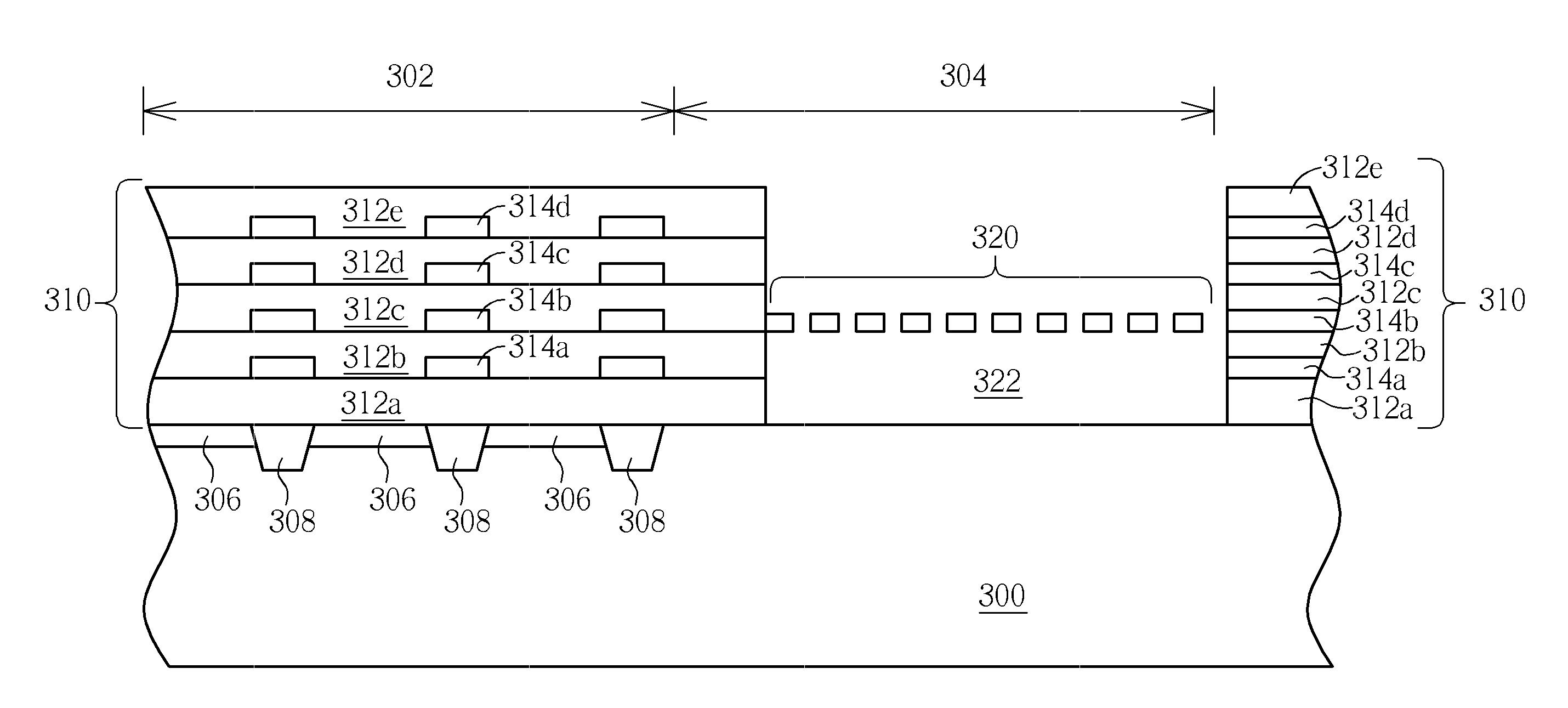
[0020]Please refer to FIGS. 3-8, which are schematic drawings illustrating the method for fabricating an integrated structure of MEMS device and CIS device provided by a first preferred embodiment of the present invention. As shown in FIG. 3, a silicon substrate 300 having a CIS region 302 and a MEMS region 304 defined therein is provided. The CIS region 302 further comprises a plurality of CIS devices such as photodiodes 306 shown in FIG. 3. Each photodiode 306 is electrically connected to a corresponding reset transistor and MOS transistors of current source follower and row selector (not shown). A plurality of shallow trench isolations (STIs) 308 is provided to electrically isolate adjacent photodiodes 306 and the MOS transistors.

[0021]Please refer to FIG. 3 again. Next, a multilevel interconnect process is performed to form a multilevel interconnect structure 310 in the CIS region 302 and the MEMS region 304 on a front side of the substrate 300. The multilevel interconnect struc...


PUM


Abstract

An integrated structure of MEMS device and CIS device and a fabricating method thereof includes providing a substrate having a CIS region and a MEMS region defined therein with a plurality of CIS devices positioned in the CIS region; performing a multilevel interconnect process to form a multilevel interconnect structure in the CIS region and the MEMS region and a micro-machined mesh metal in the MEMS region on a front side of the substrate; performing a first etching process to form a chamber in MEMS region in the front side of the substrate; forming a first mask pattern and a second mask pattern respectively in the CIS region and the MEMS region on a back side of the substrate; and performing a second etching process to form a plurality of vent holes connecting to the chamber on the back side of the substrate through the second mask pattern.

Description

BACKGROUND OF THE INVENTION[0001]1. Field of the Invention[0002]The invention relates to an integrated structure of a micro-electromechanical system (MEMS) device and a complementary metal-oxide semiconductor (CMOS) image sensor (CIS) device and a fabricating method thereof, and more particularly, to an integrated structure of MEMS microphone and CIS device and a fabricating method thereof.[0003]2. Description of the Prior Art[0004]MEMS devices are tiny 3D-structures, such as circuits, micro-sensors, and micro-actuators, formed on wafers by microminiaturization technology. Such devices are operated based on electromagnetic, electrostructive, thermoelectric, or piezoresistive effect, exemplarily. Conventionally MEMS devices are formed on insulators or other substrates by micro-electronic techniques such as photolithography, vapor deposition, and etching. Nevertheless, it is a trend to fabricate MEMS devices by processes that have been applied in fabrication of conventional analog and...

Claims


Application Information

Patent Timeline
IPC IPC(8): H01L31/00H01L21/4763H01L21/00
CPCB81C1/00246H01L27/14621H01L27/14627H01L27/14636H01L27/1464H01L27/14685H01L27/14689B81C2203/0714H01L27/14643
Inventor SHIH, HUI-SHEN
Owner UNITED MICROELECTRONICS CORP
Why Eureka
Try Eureka