
Semiconductor memory device having selective activation circuit for selectively activating circuit areas

a memory device and selective activation technology, applied in the direction of information storage, static storage, digital storage, etc., can solve the problems of not being able to control only a part of the internal circuit, the sub-threshold current of the transistor is increased in a non-conductive state, and the power consumption cannot be reduced to a satisfactory extent, so as to achieve the effect of reducing power consumption

Inactive Publication Date: 2010-06-17
ELPIDA MEMORY INC
View PDF3 Cites 29 Cited by
  • Summary
  • Abstract
  • Description
  • Claims
  • Application Information

AI Technical Summary

Benefits of technology

[0013]As described above, in the semiconductor memory device according to the present invention, a circuit area where an operation is required in response to an address signal is activated and a circuit area where the operation is not required is deactivated. Therefore, the power consumption can be reduced in the active state by a dynamic power control in response to an address signal, not by entire power control by an external command.

Problems solved by technology

However, as the operation voltage is lowered, because it is required to lower the threshold voltage in proportion to the decrease of the operation voltage, it causes a problem that the sub-threshold current of the transistor is increased in a non-conductive state.
That is, it is not possible to control to enter only a part of an internal circuit in the standby state and to disconnect the main power source line and the sub power source line only in the corresponding circuit portion.
Therefore, the power consumption cannot be reduced to a satisfactory extent, and a semiconductor memory device that can further reduce the power consumption has been desired.

Method used


Image

  • Semiconductor memory device having selective activation circuit for selectively activating circuit areas
  • Semiconductor memory device having selective activation circuit for selectively activating circuit areas
  • Semiconductor memory device having selective activation circuit for selectively activating circuit areas

Examples


first embodiment

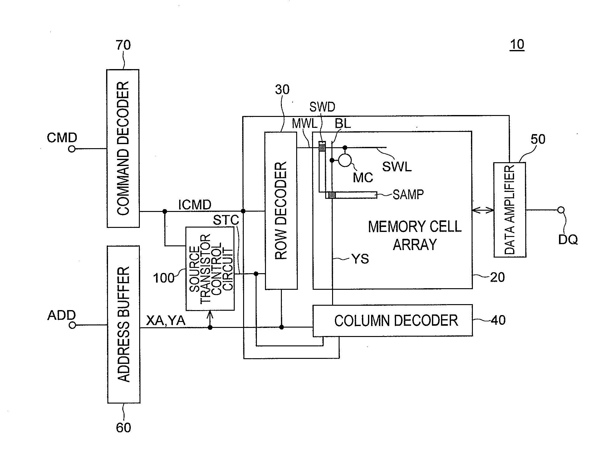
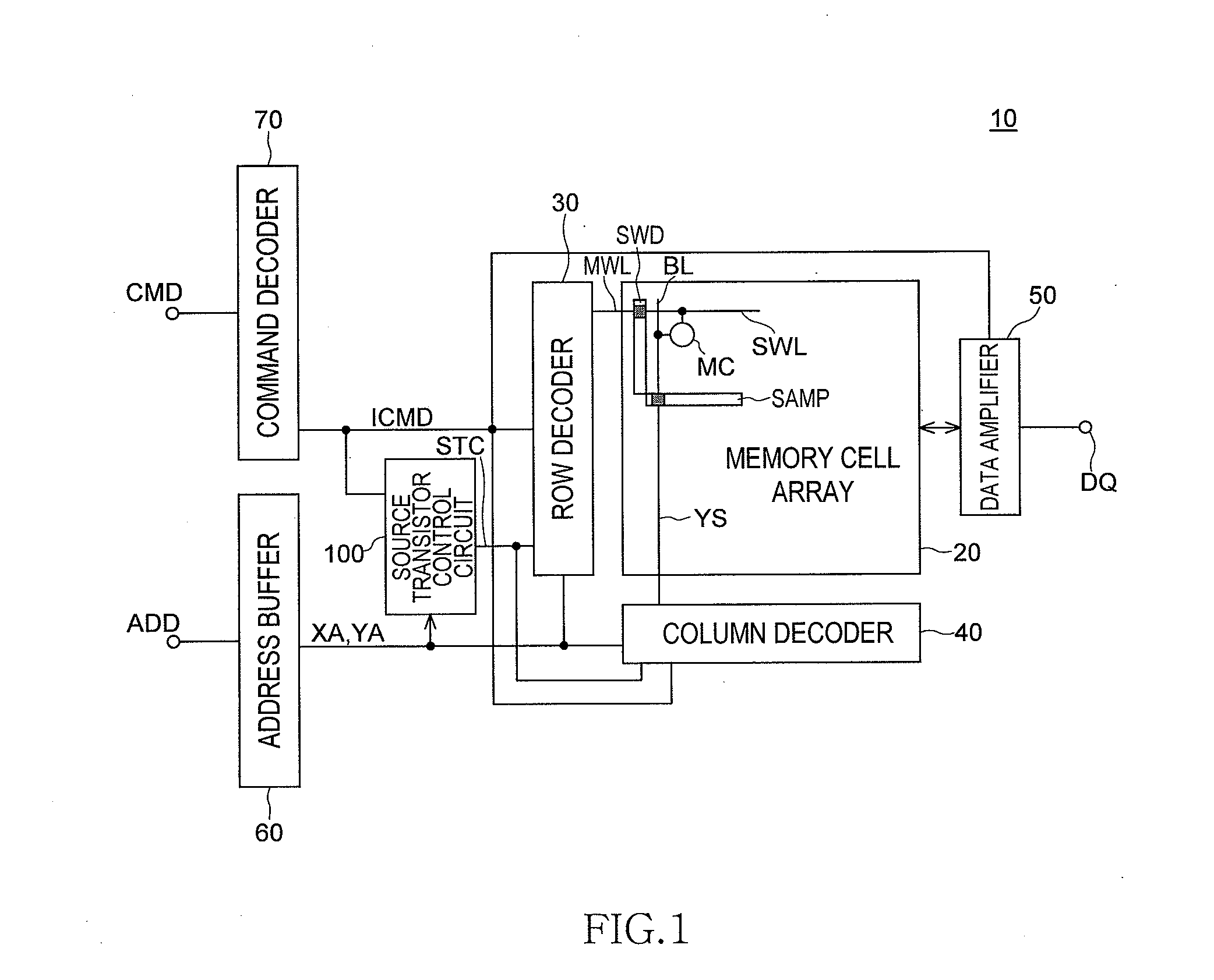
[0030]FIG. 1 is an overall block diagram of a semiconductor memory device 10 according to the present invention.

[0031]As shown in FIG. 1, the semiconductor memory device 10 includes a memory cell array 20 that includes a plurality of memory cells, a row decoder 30 that performs a row access to the memory cell array 20, and a column decoder 40 that performs a column access to the memory cell array 20. The memory cell array 20 includes a sub-word line SWL, a bit line BL, and a memory cell MC that is connected to the sub-word line SWL and the bit line BL. The sub-word line SWL is connected to a sub-word driver SWD that is controlled by a main-word signal on a main-word line MWL. The bit line BL is connected to a sense amplifier SAMP that is selected by a column selection signal on a column selection line YS. Selection of the main-word line MWL and the sub-word line SWL is performed by the row decoder 30 based on a row address signal XA. Selection of the column selection line YS and the...

second embodiment

[0075]the present invention is explained next.

[0076]FIG. 11 is an enlarged block diagram of a memory bank 21 according to the second embodiment showing its main parts, and FIG. 11 corresponds to FIG. 3 for explaining the first embodiment.

[0077]As shown in FIG. 11, the second embodiment is different from the first embodiment in that the source transistor control circuit 100 includes an SR latch circuit 110 and an output of the SR latch circuit 110 is the source transistor control signal STC1. Other features of the second embodiment are identical to those of the first embedment, and thus explanations thereof will be omitted.

[0078]An internal signal RASB is supplied to a set-side input terminal S of the SR latch circuit 110 via a pulse generating circuit 120. The internal signal RASB is a signal that becomes a Low level in response to issuance of an active command. Therefore, when the active command is issued, the SR latch circuit 110 is set, by which the source transistor control sign...

third embodiment

[0086]FIG. 14 is a block diagram of a semiconductor memory device according to the present invention.

[0087]In the third embodiment, as shown in FIG. 14, a source transistor control signal STC1 is supplied to a column select circuit group 41 that constitutes the column decoder 40. The column select circuit group 41 includes a plurality of column select circuits 400, 401, . . . , which are selected based on their corresponding pre-decode signals PY0, PY1, . . . . The pre-decode signals PY0, PY1, . . . are signals generated by pre-decoding a part of the column address YA by a column pre-decoder 42. The column select circuit group 41 and the column pre-decoder 42 form the column decoder 40 shown in FIG. 1.

[0088]In the above configuration, the column select circuits 400, 401, . . . are selectively activated based on the source transistor control signal STC1 and the pre-decode signals PY0, PY1, . . . , as it is in the first and second embodiments. Therefore, only a column select circuit t...


PUM


Abstract

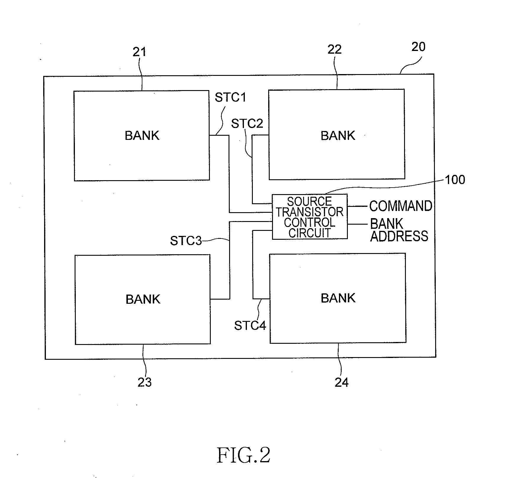
A semiconductor memory device includes a plurality of memory banks each including a plurality of circuit areas selected based on an address signal, any one of which is selected by a corresponding bank selective signal (source transistor control signals), and a selective activation circuit that, from among circuit areas included in a memory bank that is selected based on the bank selective signal, activates any one of the circuit areas based on the address signal, and deactivates at least one of rest of the circuit areas. According to the present invention, the power consumption can be reduced in an active state by a dynamic power control in response to an address signal, not by entire power control by an external command.

Description

BACKGROUND OF THE INVENTION[0001]1. Field of the Invention[0002]The present invention relates to a semiconductor memory device, and particularly relates to a semiconductor memory device in which power consumption is reduced.[0003]2. Description of Related Art[0004]In recent years, the operation voltage of a semiconductor device is gradually lowered in order to reduce its power consumption. At present, a considerably low operation voltage on the order of 1 volt is often used. However, as the operation voltage is lowered, because it is required to lower the threshold voltage in proportion to the decrease of the operation voltage, it causes a problem that the sub-threshold current of the transistor is increased in a non-conductive state.[0005]To deal with such problems, there has been proposed a method for a semiconductor device disclosed in Japanese Patent Application Laid-open No. H11-31385, which has a structure in which a power source line of a circuit area where logic is fixed at ...

Claims


Application Information

Patent Timeline
IPC IPC(8): G11C8/00G11C8/08
CPCG11C8/08G11C11/408G11C11/4076G11C11/4074
Inventor KITAYAMA, MAKOTO
Owner ELPIDA MEMORY INC
Learn More