Digital alloy absorber for photodetectors

Active Publication Date: 2010-06-24
CALIFORNIA INST OF TECH
View PDF8 Cites 37 Cited by
  • Summary
  • Abstract
  • Description
  • Claims
  • Application Information

AI Technical Summary

Benefits of technology

[0020]In order to increase the spectral response range and improve the mobility of the photo-generated carriers (e.g. in an nBn photodetector), a digital alloy absorber may be employed by embedding one (or fraction thereof) to several monolayers of a semiconductor material (insert layers) periodically into a different host semiconductor material of the absorber layer. The semiconductor material of the insert layer and the host semiconductor materials may have lattice constants that are substantial

Problems solved by technology

Although the depletion layer enhances detector performance in this manner, it also introduces Shockley-Read-Hall (SRH) dark currents which introduce noise.
The resulting dark current limits the operating temperature.
However, specific designs of barrier ph

Method used


Image

  • Digital alloy absorber for photodetectors
  • Digital alloy absorber for photodetectors
  • Digital alloy absorber for photodetectors

Examples


Embodiment Construction

1. Overview

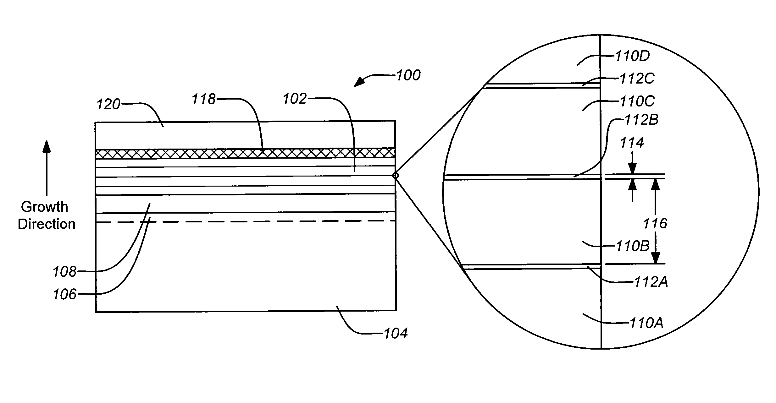
[0036]As previously mentioned, embodiments of the present invention are directed to a novel digital alloy absorber layer for semiconductor photodetectors which can increase the spectral response range and improve the mobility of the photo-generated carriers (e.g. in an nBn photodetector or a p-n photodetector). A digital alloy absorber embodiment of the invention can employ one (or fraction thereof) to several monolayers of a semiconductor (insert layers) periodically embedded into a different host semiconductor material of the absorber layer. The semiconductor material of the insert layer(s) and the host semiconductor material may have lattice constants that are substantially mismatched. The described technique simultaneously allows for control of alloy composition and net strain, which are both key parameters for the photodetector operation.

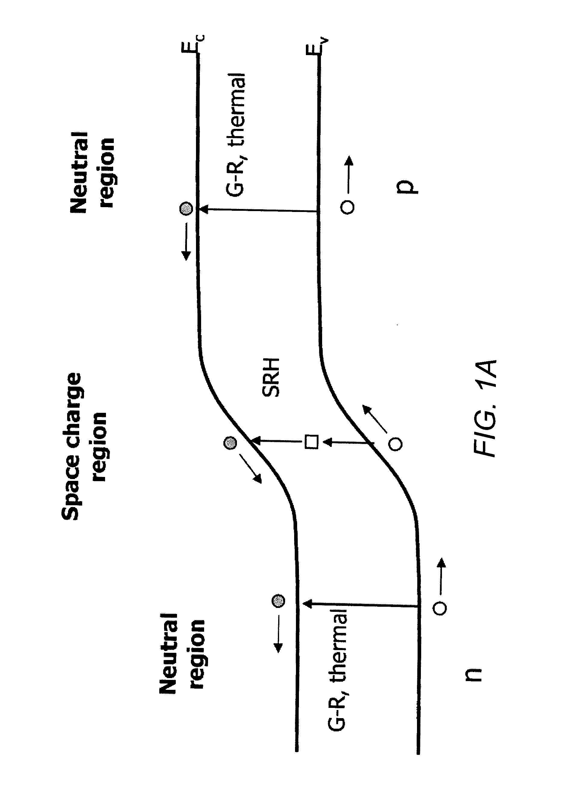
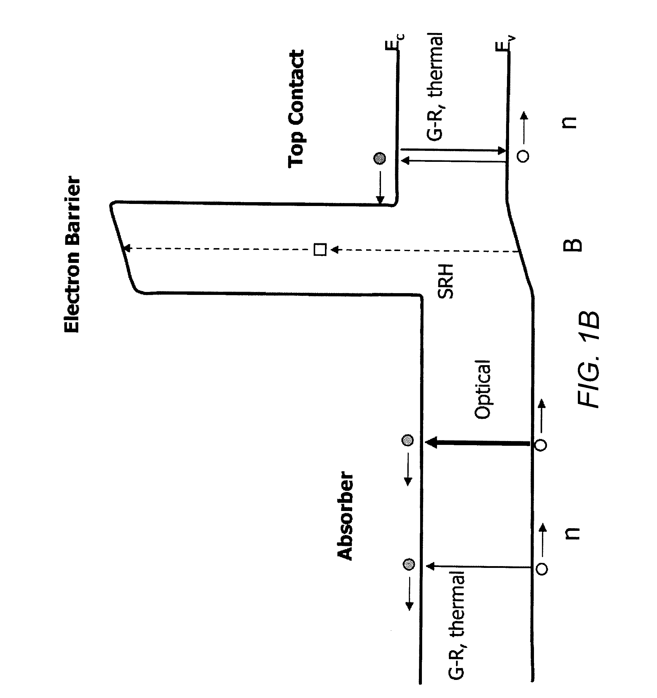
[0037]In an nBn photodetector, the absorber is doped n-type, and therefore its photocarrier extraction property depends largely on ...


PUM


Abstract

In order to increase the spectral response range and improve the mobility of the photo-generated carriers (e.g. in an nBn photodetector), a digital alloy absorber may be employed by embedding one (or fraction thereof) to several monolayers of a semiconductor material (insert layers) periodically into a different host semiconductor material of the absorber layer. The semiconductor material of the insert layer and the host semiconductor materials may have lattice constants that are substantially mismatched. For example, this may performed by periodically embedding monolayers of InSb into an InAsSb host as the absorption region to extend the cutoff wavelength of InAsSb photodetectors, such as InAsSb based nBn devices. The described technique allows for simultaneous control of alloy composition and net strain, which are both key parameters for the photodetector operation.

Description

CROSS-REFERENCE TO RELATED APPLICATIONS[0001]This application claims the benefit under 35 U.S.C. §119(e) of the following U.S. provisional patent application, which is incorporated by reference herein:[0002]U.S. Provisional Patent Application No. 61 / 201,849, filed Dec. 16, 2008, and entitled “DIGITAL ALLOY METHOD FOR IMPROVED NBN DETECTORS”, by Hill et al. (Attorney Docket CIT-5280-P).[0003]This application is related to U.S. patent application Ser. No. 12 / 567,635, filed Sep. 25, 2009 by Ting et al., and entitled “HIGH OPERATING TEMPERATURE BARRIER INFRARED DETECTOR WITH TAILORABLE CUTOFF WAVELENGTH,” which is incorporated by reference herein.STATEMENT OF GOVERNMENT RIGHTS[0004]The invention described herein was made in the performance of work under a NASA contract, and is subject to the provisions of Public Law 96-517 (35 USC 202) in which the Contractor has elected to retain title.BACKGROUND OF THE INVENTION[0005]1. Field of the Invention[0006]This invention relates to photodetect...

Claims


Application Information

Patent Timeline
IPC IPC(8): H01L31/0304
CPCH01L31/03046H01L31/101Y02E10/544
Inventor HILL, CORY J.TING, DAVID Z.GUNAPALA, SARATH D.
Owner CALIFORNIA INST OF TECH
Why Eureka
Try Eureka