MEMS process and device

a technology of mems and process, applied in the direction of instruments, open-end spinning machines, loudspeaker diaphragm shapes, etc., can solve the problems of interference, noise, parasitic capacitance and inductance, and difficulty in achieving compatibility with the standard process used to fabricate complementary metal-oxide-semiconductor (cmos) electronic devices during the manufacture of mems devices

Active Publication Date: 2010-06-24
CIRRUS LOGIC INC
View PDF24 Cites 40 Cited by
  • Summary
  • Abstract
  • Description
  • Claims
  • Application Information

AI Technical Summary

Benefits of technology

[0013]The provision of first and second sacrificial layers has a number of advantages. First, the sacrificial layers help protect the membrane during other fabrication steps. Secondly, the first and second sacrificial layers enable the size of the membrane to be formed independent of a subsequent back etch process.

Problems solved by technology

One of the challenges in reaching these goals is the difficulty of achieving compatibility with standard processes used to fabricate complementary-metal-oxide-semiconductor (CMOS) electronic devices during manufacture of MEMS devices.
A disadvantage of the process described above is that the back-etch is difficult to perform in an accurate manner when using a wet-etch or a dry-etch.
However, this can lead to problems with interference, noise and parasitic capacitance and inductance.
As a result, the devices can be fragile and may be damaged during singulation.
All of these dicing methods have associated problems when applied to MEMS structures.
This produces a slurry from the water and abraded pieces of wafer that may penetrate any open part of the MEMS structure and render it useless, as it is difficult to clean the slurry out at a later stage due to the small size of the singulated devices.
Additionally, the lubricating coolant may be sprayed onto the wafer at high speed thus placing any delicate sensor structure under high mechanical stress and potentially damaging it.
Laser singulation is slightly cleaner than blade dicing but is more expensive.
However, the heating produced by the cutting process may set up thermal gradients leading to areas of different thermal expansion in the sensor structures that may distort them and render them useless.
Also the laser singulation process produces some residue that may clog any open structure and prevent the device from operating properly.

Method used


Image

  • MEMS process and device
  • MEMS process and device
  • MEMS process and device

Examples


Embodiment Construction

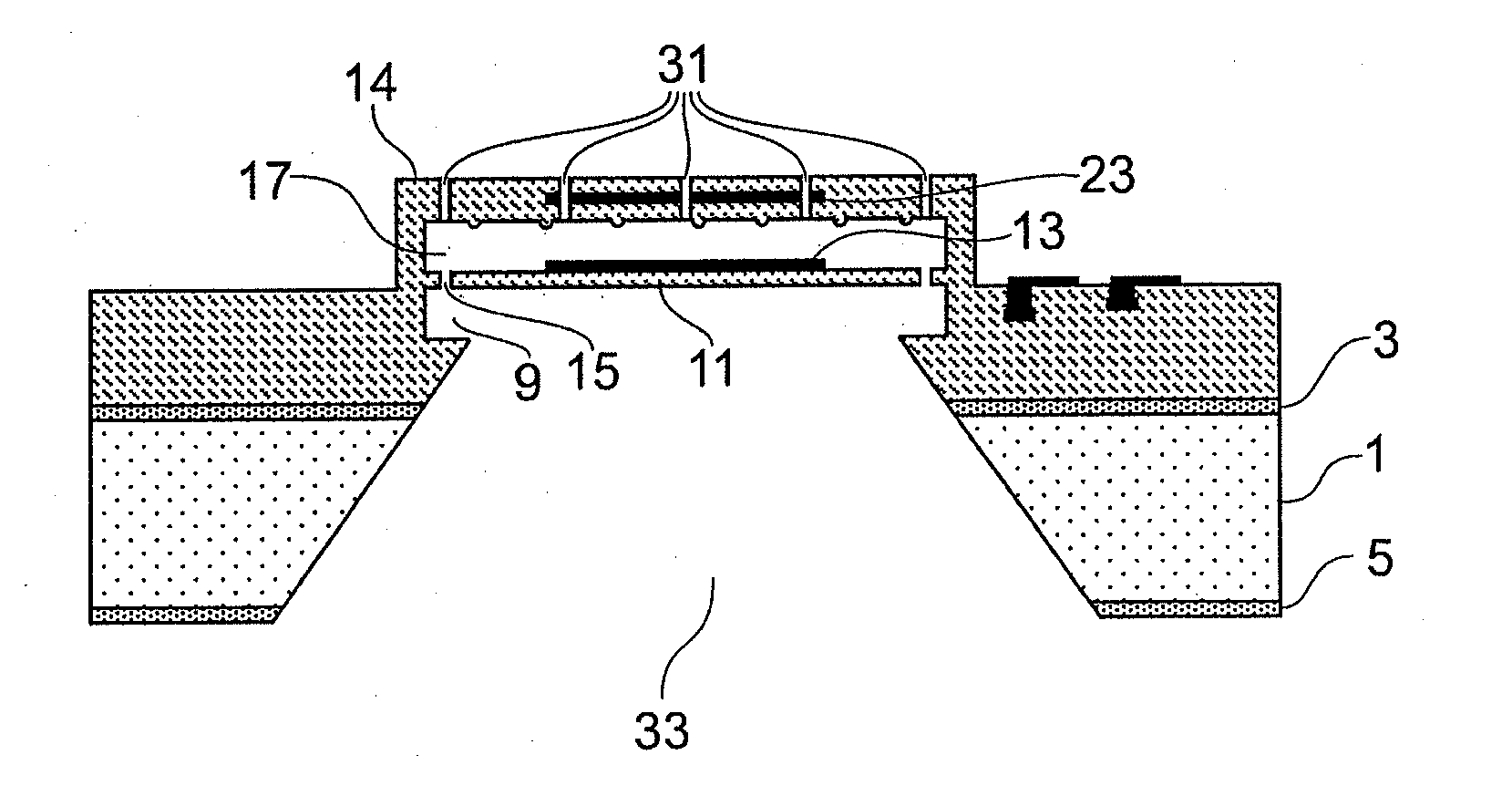
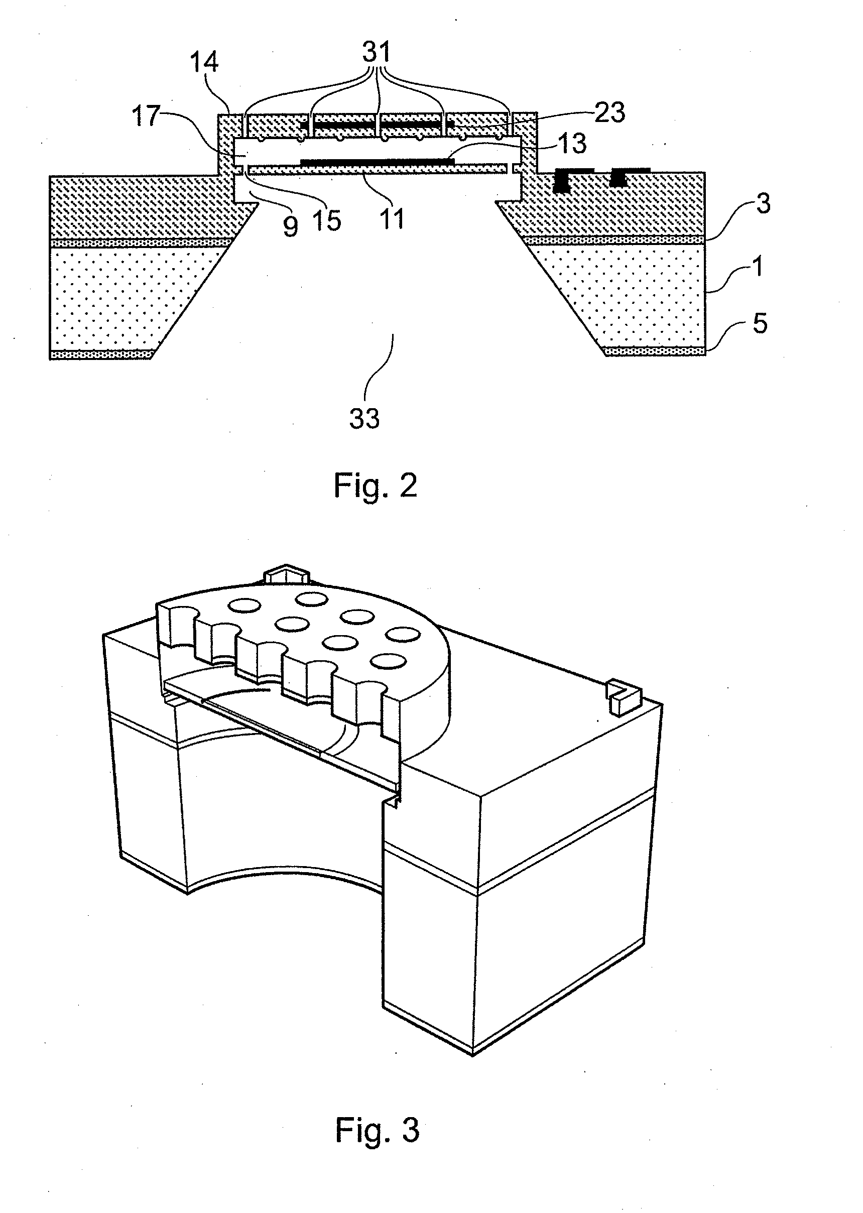
[0027]FIGS. 2 and 3 show a schematic diagram and a perspective view, respectively, of a capacitive microphone device according to the present invention. The capacitive microphone device comprises a flexible membrane 11 that is free to move in response to pressure differences generated by sound waves. A first electrode 13 is mechanically coupled to the flexible membrane 11, and together they form a first capacitive plate of the capacitive microphone device. A second electrode 23 is mechanically coupled to a generally rigid structural layer or back-plate 14, which together form a second capacitive plate of the capacitive microphone device.

[0028]The capacitive microphone is formed on a substrate 1, for example a silicon wafer. A back-volume 33 is provided below the membrane 11, and is formed using a “back-etch” through the substrate 1, as will be described in greater detail later in the application. A first cavity 9 is located directly below the membrane 11. The first cavity 9 is forme...


PUM

PropertyMeasurementUnit
frequencyaaaaaaaaaa
thicknessaaaaaaaaaa
thicknessaaaaaaaaaa

Abstract

A MEMS device, for example a capacitive microphone, comprises a flexible membrane 11 that is free to move in response to pressure differences generated by sound waves. A first electrode 13 is mechanically coupled to the flexible membrane 11, and together form a first capacitive plate of the capacitive microphone device. A second electrode 23 is mechanically coupled to a generally rigid structural layer or back-plate 14, which together form a second capacitive plate of the capacitive microphone device. The capacitive microphone is formed on a substrate 1, for example a silicon wafer. A back-volume 33 is provided below the membrane 11, and is formed using a “back-etch” through the substrate 1. A first cavity 9 is located directly below the membrane 11, and is formed using a first sacrificial layer during the fabrication process. Interposed between the first and second electrodes 13 and 23 is a second cavity 17, which is formed using a second sacrificial layer during the fabrication process. A plurality of bleed holes 15 connect the first cavity 9 and the second cavity 17. Acoustic holes 31 are arranged in the back-plate 14 so as to allow free movement of air molecules, such that the sound waves can enter the second cavity 17. The first and second cavities 9 and 17 in association with the back-volume 33 allow the membrane 11 to move in response to the sound waves entering via the acoustic holes 31 in the back-plate 14. The provision of first and second sacrificial layers has the advantage of protecting the membrane during manufacture, and disassociating the back etch process from the definition of the membrane. The bleed holes 15 aid with the removal of the first and second sacrificial layers. The bleed holes 15 also contribute to the operating characteristics of the microphone.

Description

FIELD OF THE INVENTION[0001]This invention relates to a MEMS process and device, and in particular to a MEMS process and device relating to a transducer, and in particular a capacitive microphone.BACKGROUND OF THE INVENTION[0002]Consumer electronics devices are continually getting smaller and, with advances in technology, are gaining ever increasing performance and functionality. This is clearly evident in the technology used in consumer electronic products such as mobile phones, laptop computers, MP3 players and personal digital assistants (PDAs). Requirements of the mobile phone industry for example, are driving the components to become smaller with higher functionality and reduced cost. It is therefore desirable to integrate functions of electronic circuits together and combine them with transducer devices such as microphones and speakers.[0003]The result of this is the emergence of micro-electrical-mechanical-systems (MEMS) based transducer devices. These may be for example, cap...

Claims


Application Information

Patent Timeline
Patent Type & Authority Applications(United States)
IPC IPC(8): H01L29/84
CPCB81B2201/0257B81B2203/0127B81C1/00158B81C99/004Y10S977/733H04R7/10H04R7/18H04R19/005H04R2307/207B81C2201/0109H04R19/016H04R19/04B81B3/00B81B3/0021B81C1/00182B81B3/0027B81B2201/07B81B2201/02B81B2201/0271B81B2201/0264
Inventor LAMING, RICHARD I.BEGBIE, MARKTRAYNOR, ANTHONY
Owner CIRRUS LOGIC INC
Why Eureka
Try Eureka