Stamper for transferring fine pattern and method for manufacturing thereof

a technology of transfer and fine pattern, which is applied in the direction of manufacturing tools, photomechanical equipment, instruments, etc., can solve the problems of increasing exposure time (drawing time), shrinking of fine pattern, and difficult processing of fine pattern by photolithography technology

Inactive Publication Date: 2010-06-24
HITACHI HIGH-TECH CORP
View PDF4 Cites 39 Cited by
  • Summary
  • Abstract
  • Description
  • Claims
  • Application Information

AI Technical Summary

Problems solved by technology

Because, however, the pattern has been shrunk and a required process dimension has been shrunk as small as a light source wave length which is used for an exposure, it becomes difficult to process the fine pattern by the photolithography technology.
Therefore, there is a disadvantage that an exposure time (drawing time) increases as a number of patterns to be drawn increases.
Accordingly, a long time is required for completing the patterns.
As a result, in proportion to a degree of integration of a semiconductor integrated circuit, a time required for the pattern formation increases, thereby resulting in reduction of a throughput.
However, because a degree of requirement for fine pattern has progres

Method used


Image

  • Stamper for transferring fine pattern and method for manufacturing thereof
  • Stamper for transferring fine pattern and method for manufacturing thereof
  • Stamper for transferring fine pattern and method for manufacturing thereof

Examples


embodiments

[0055]Next, the present invention will be explained more specifically with reference to the following examples. In the following explanations, units “phr (per hundred resin)” and “%” are based on weight unless otherwise stated.

example 1

[0056]First, a silsesquioxane derivative OX-SQ SI-20 (Toagosei Limited) (1 phr) having a plurality of oxetanyl groups is mixed with an Adeka OPTOMER SP-172 (Asahi Denka Corporation) (0.06 phr) which is a cationic polymerization initiator in order to prepare a photo-curable resinous compound of a fine structure layer.

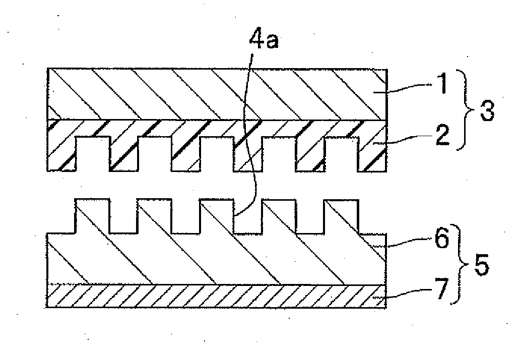
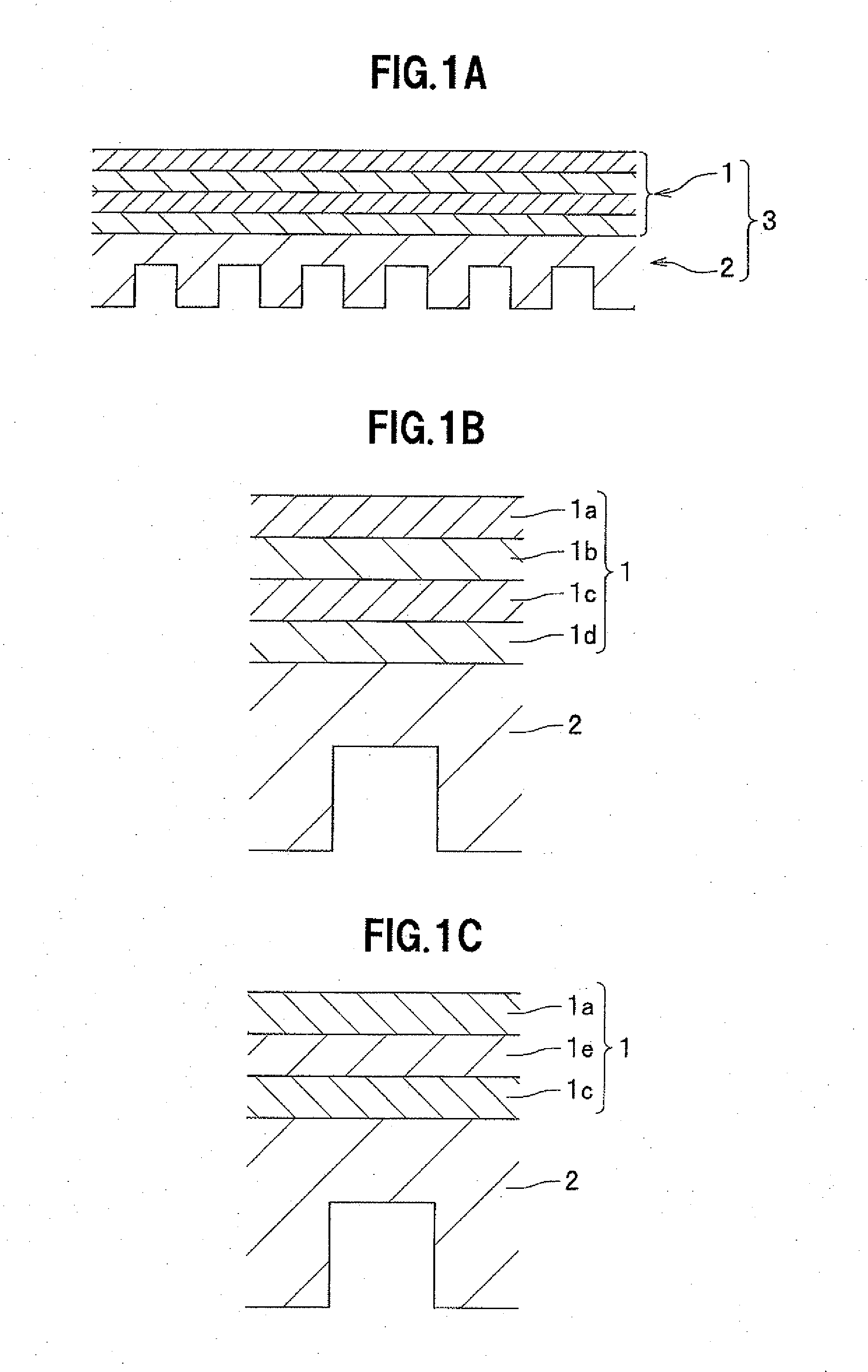
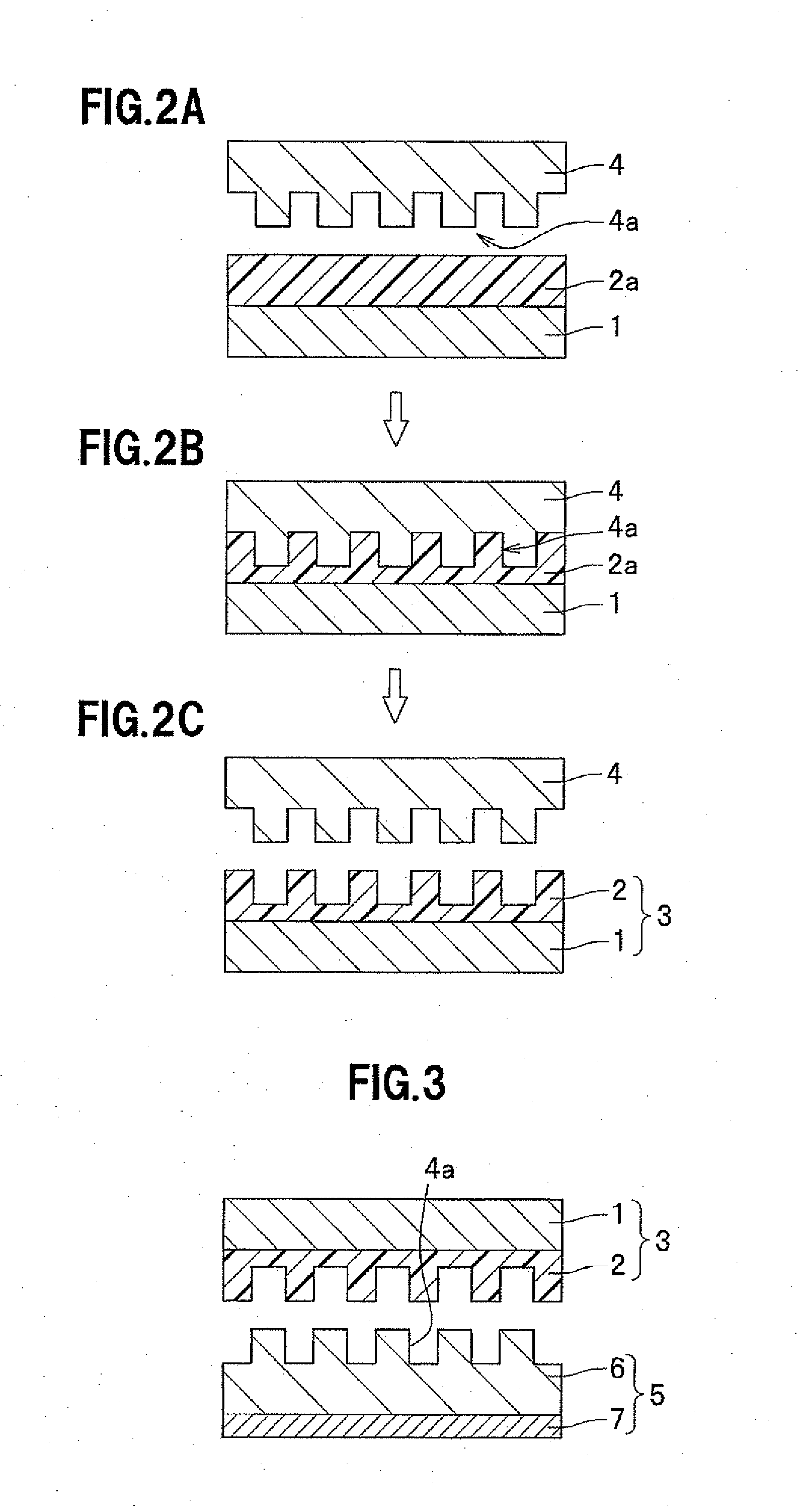
[0057]Next, a supporting substrate (20 millimeters*20 millimeters, 0.7 millimeters thick) whose surface is coupling-treated with a KBM403 (Shin-Etsu Silicones Co., Ltd.) is prepared. A resinous compound which will be a fine structure layer is dropped on the coupling-treated surface of the supporting substrate. Next, a ultraviolet light having wavelength of 365 nanometers is irradiated for 120 seconds with a quartz master mold, in which hole patterns (180 nanometers in diameter, 180 nanometers in spacing, and 200 nanometers in height) are formed on a releasing-treated surface with a OPTOOL DSX (Daikin Industries, Ltd.), being pressed against the photo-curable resinous com...

example 2

[0058]The stamper having the fine structure layer is manufactured by a similar method to that described in Example 1. At that time, a silsesquioxane derivative Q-4OG (Toagosei Limited) (1 phr) having eight epoxy groups is mixed with the Adeka OPTOMER SP-172 (Asahi Denka Corporation) (0.06 phr) which is the cationic polymerization initiator in order to manufacture the photo-curable resinous compound of the fine structure layer. Using this photo-curable resinous compound, by the similar method to that described in Example 1, the stamper is manufactured, continuous transferring is performed, measurement is performed by AFM, and an error is evaluated. A maximum dimensional-error in height of the fine structure pattern after 50 times transferring is on the order of 3%, and accurate and continuous transferring can be performed by the stamper without releasing treatment.


PUM

PropertyMeasurementUnit
Percent by massaaaaaaaaaa
Elasticityaaaaaaaaaa
Lightaaaaaaaaaa

Abstract

An object of the present invention is to provide a stamper for transferring fine pattern and a method for manufacturing the stamper, the stamper has a fine structure layer to improve a continuous transferring property of the resinous stamper, and to allow accurate and continuous transferring. In order to achieve the above object, the present invention provides a stamper for transferring fine pattern, including: a fine structure layer on a supporting substrate, in which the fine structure layer is a polymer of a resinous compound whose principal component is silsesquioxane derivative having a plurality of polymerizable functional groups.

Description

CROSS REFERENCE TO RELATED APPLICATIONS[0001]The present application claims benefit of the filing date of Japanese Patent Application No. 2008-315142 filed on Dec. 11, 2008 which is incorporated herein by reference.FIELD OF THE INVENTION[0002]The present invention relates to a stamper for transferring a fine pattern on a surface of a transferred object by pressing the stamper against the surface, and to a method for manufacturing the stamper.DESCRIPTION OF THE RELATED ART[0003]Conventionally, a photolithography technology is frequently used as the technology for processing a fine pattern needed in semiconductor devices, etc. Because, however, the pattern has been shrunk and a required process dimension has been shrunk as small as a light source wave length which is used for an exposure, it becomes difficult to process the fine pattern by the photolithography technology. For this reason, instead of the photolithography technology, an electron beam lithography apparatus which is a kin...

Claims


Application Information

Patent Timeline
IPC IPC(8): B29C59/16B28B1/10
CPCB29C35/02B29C35/0888B29C59/022G03F7/0002B29C2059/023B82Y10/00B82Y40/00B29C2035/0827
Inventor ISHII, SATOSHIOGINO, MASAHIKOSHIZAWA, NORITAKEMORI, KYOICHIMIYAUCHI, AKIHIRO
Owner HITACHI HIGH-TECH CORP
Why Eureka
Try Eureka