

Ultra-fine microfabrication method using an energy beam
a microfabrication and ultra-fine technology, applied in the manufacture of electrode systems, electric discharge tubes/lamps, instruments, etc., can solve the problems of inability to adapt the technique to microfabrication in the nanometer range, high capital and labor expenses associated with the technique, and special equipment and effort required
- Summary
- Abstract
- Description
- Claims
- Application Information
AI Technical Summary
Benefits of technology
Problems solved by technology
Method used
Image

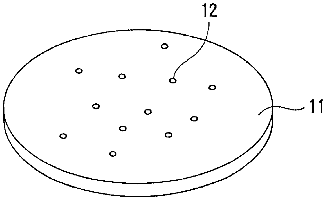
Examples
first embodiment
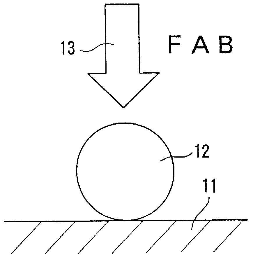
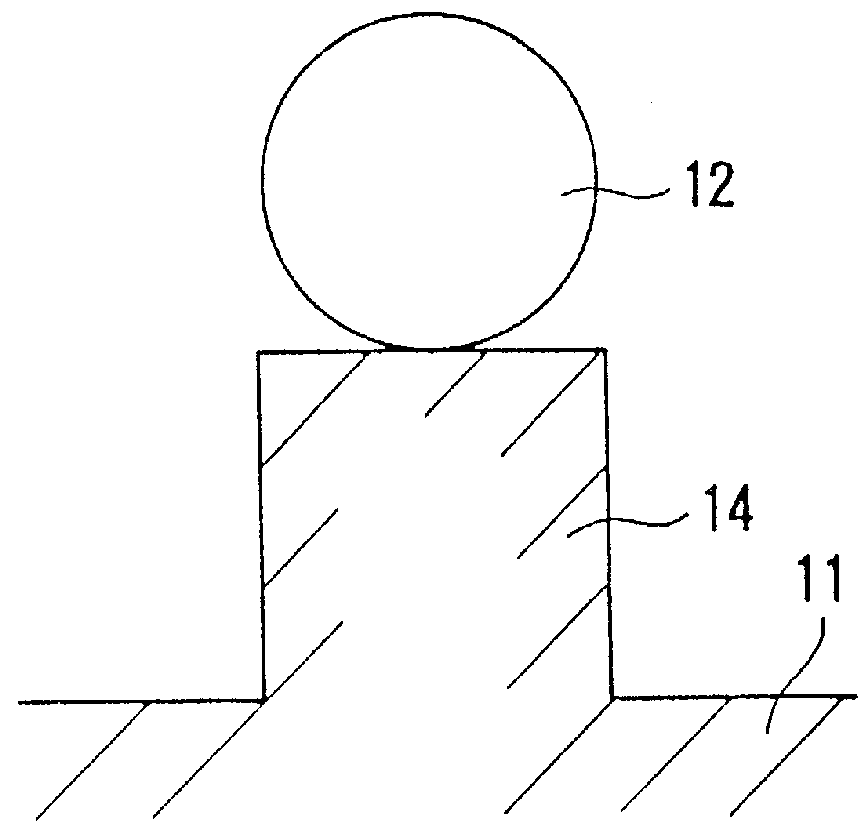
FIGS. 3A-3E illustrate the processing steps in a second method of the microfabrication method. In the first embodiment the energy beam used was a fast atomic beam 13 of a rare gas or a gas which has a high reactivity with the base material but a low reactivity with the micro-particles to suppress the etching action on the micro-particles 12. FIGS. 3A-3E present a slightly different aspect of the microfabrication method. In this case, some allowance is made for the shape change (shrinking) in the micro-particles, and the target object 21 in this case is one of III-V group semiconductor materials, such as one of GaAs, AlGaAs, InAs. Fast atomic beam (FAB) 23 is gaseous chlorine, and the micro-particles 22 are nano-particles of diamond of a particle size between 1 to 50 nm which are reactive with the FAB 23.
First, as shown in FIG. 3A, diamond nano-particles 22 are dispersed on the surface of target object 21, and FAB 23 of gaseous chlorine is directed as shown by the arrow in FIG. 3A. T...
second embodiment
The fabrication target material 60 shown in FIG. 7 is made on a silicon substrate base 61 in accordance with the steps presented in the second embodiment described above. Because the base material is silicon, the energy beam utilized is a fast atomic beam based on gaseous particles from a fluorine group, such as SF.sub.6. Isotropical fabrication is performed in a post-FAB processing step, by producing a plasma of fluorine-group gas particles, and supplying a high concentration of fluorine radicals to the fabrication surface. The cone-shaped Si fine structure 64 thus produced can be used as a cantilever needle point in an atomic field microscope (AFM) or scanning tunnelling microscope (STM). The needle tip is used to examine the surface roughness configuration of a target object, based on the vertical movement of the needle tip moving along the surface. Because of the sharpness of the needle tip of the fine structure 64, it can make concentration of an electric field easy, and can, t...
PUM
| Property | Measurement | Unit |
|---|---|---|
| particle size | aaaaa | aaaaa |
| particle size | aaaaa | aaaaa |
| size | aaaaa | aaaaa |
Abstract
Description
Claims
Application Information