Balancing A Signal Margin Of A Resistance Based Memory Circuit

a resistance based memory and signal margin technology, applied in the direction of information storage, static storage, digital storage, etc., can solve the problems of increasing noise and process variation, power consumption of portable computing devices such as portable devices can quickly deplete batteries, and user experience can be eroded, so as to improve the tolerance improve the operation of resistance based memory, and increase the signal margin

Active Publication Date: 2010-06-24
QUALCOMM INC +1
View PDF4 Cites 30 Cited by
  • Summary
  • Abstract
  • Description
  • Claims
  • Application Information

AI Technical Summary

Benefits of technology

[0009]One particular advantage provided by at least one of the disclosed embodiments is that operation of a resistance based memory may be improved by increasing a signal margin of the resistance based memory. The increased signal margin may improve a tolerance of the resistance based memory to noise or to process variation during read operations. Improved signal margin may also lead to improved memory device yield.

Problems solved by technology

However, power consumption of such portable computing devices can quickly deplete a battery and diminish a user's experience.
Reducing power consumption has led to smaller circuitry feature sizes and operating voltages within such portable devices.
Such increased sensitivity to noise and process variations may be difficult to overcome when designing memory devices that use sense amplifiers.

Method used


Image

  • Balancing A Signal Margin Of A Resistance Based Memory Circuit
  • Balancing A Signal Margin Of A Resistance Based Memory Circuit
  • Balancing A Signal Margin Of A Resistance Based Memory Circuit

Examples


Embodiment Construction

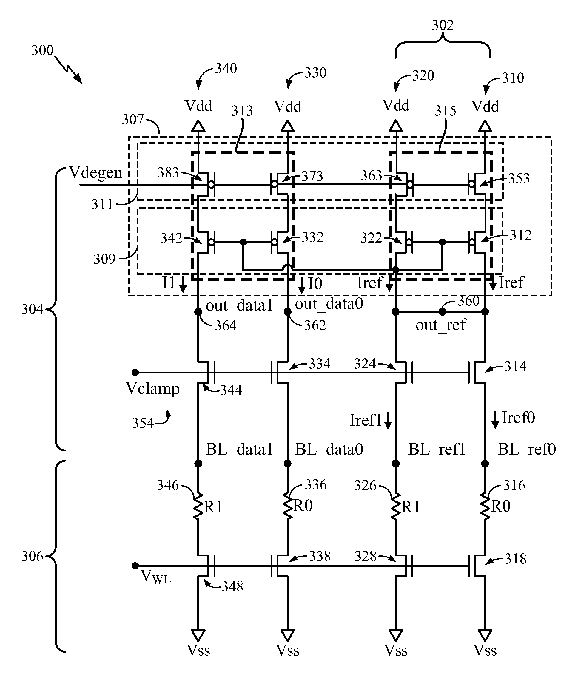
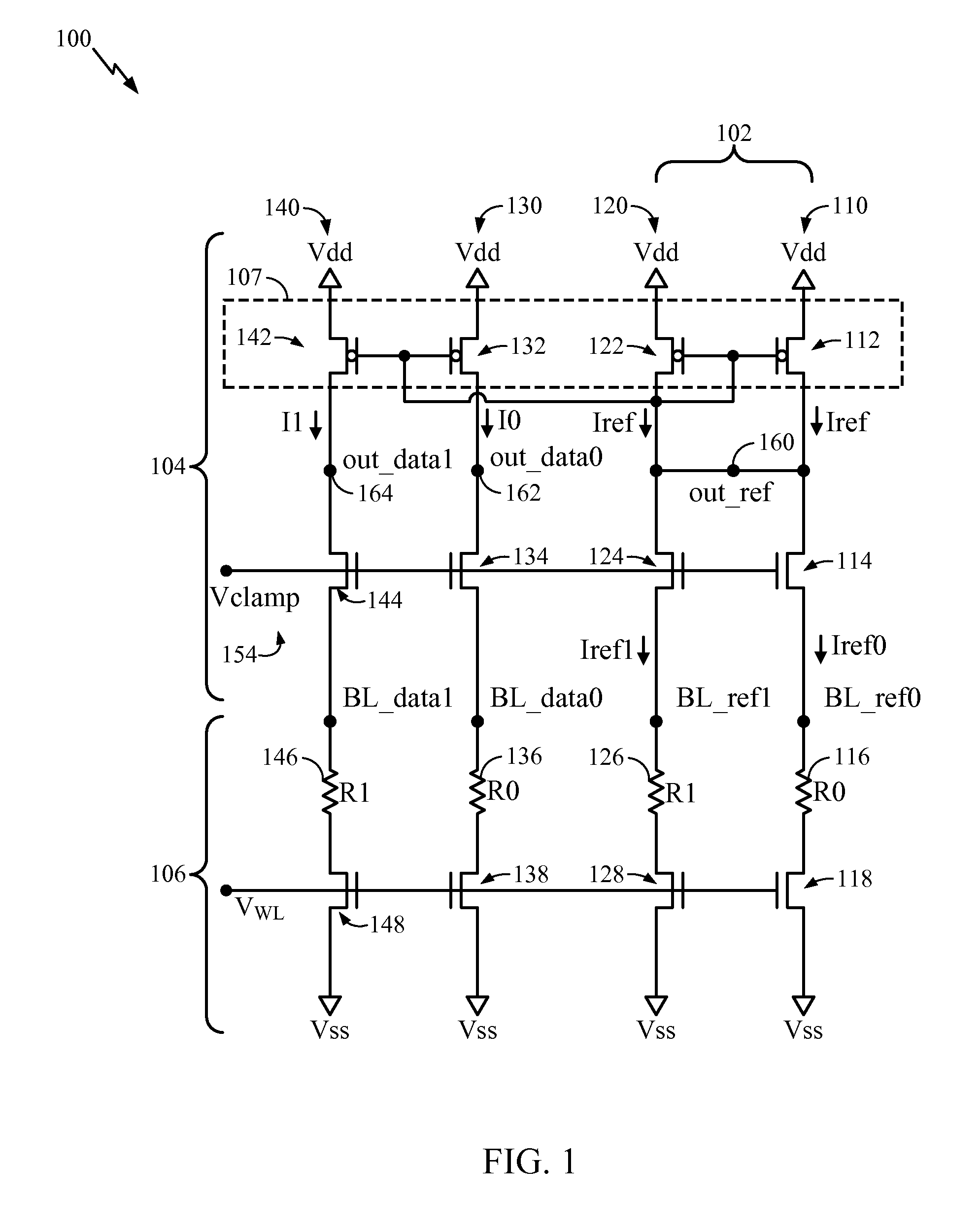
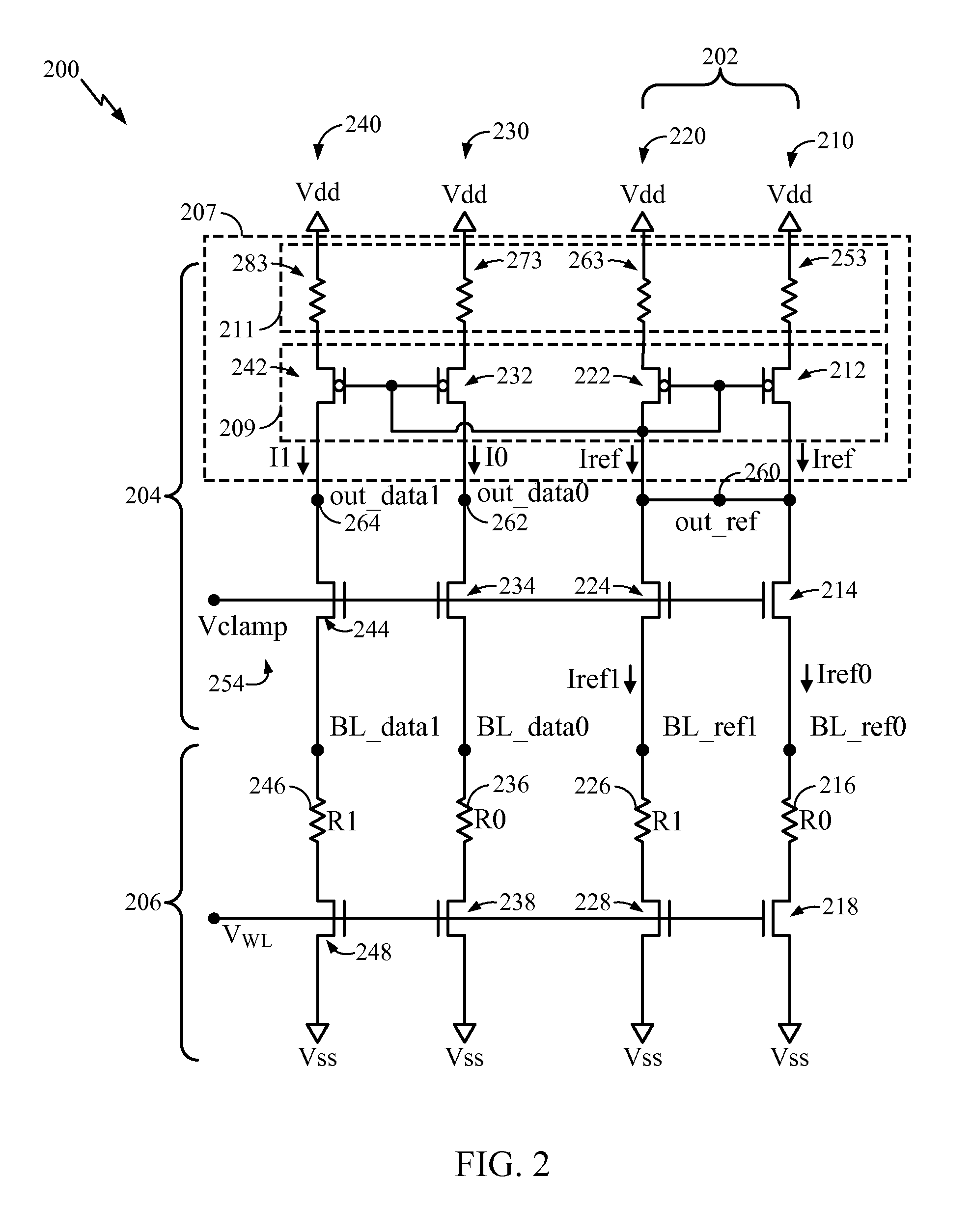
[0024]Referring to FIG. 1, a particular illustrative embodiment of a resistance based memory including a transistor load 107 is depicted and generally designated 100. The memory 100 includes a reference circuit 102 having a first reference path 110 and a second reference path 120. The memory 100 also includes a representative logic bit-zero data path 130 and a representative logic bit-one data path 140. The representative logic bit-zero data path 130 includes a first bit line adapted to read a logic zero value, and the representative logic bit-one data path 140 includes a second bit line adapted to read a logic one value. Transistor load 107 is coupled to the first bit line, to the second bit line, and to reference paths 110 and 120. The reference paths 110 and 120 and the data paths 130 and 140 are generally designated as having a sense amplifier portion 104 that provides load elements to a memory cell portion 106 to generate an output signal for comparison at a second sense amplif...


PUM


Abstract

A resistance based memory circuit is disclosed. The circuit includes a first transistor load of a data cell and a bit line adapted to detect a first logic state. The bit line is coupled to the first transistor load and coupled to a data cell having a magnetic tunnel junction (MTJ) structure. The bit line is adapted to detect data having a logic one value when the bit line has a first voltage value, and to detect data having a logic zero value when the bit line has a second voltage value. The circuit further includes a second transistor load of a reference cell. The second transistor load is coupled to the first transistor load, and the second transistor load has an associated reference voltage value. A characteristic of the first transistor load, such as transistor width, is adjustable to modify the first voltage value and the second voltage value without substantially changing the reference voltage value.

Description

FIELD [0001]The present disclosure is generally related to source degeneration and balancing a signal margin of a resistance based memory circuit.DESCRIPTION OF RELATED ART [0002]Advances in technology have resulted in smaller and more powerful personal computing devices. For example, there currently exist a variety of portable computing devices, including wireless computing devices, such as portable wireless telephones, personal digital assistants (PDAs), and paging devices that are small, lightweight, and easily carried by users. More specifically, portable wireless telephones, such as cellular telephones and internet protocol (IP) telephones, can communicate voice and data packets over wireless networks. Further, many such wireless telephones include other types of devices that are incorporated therein. For example, a wireless telephone can also include a digital still camera, a digital video camera, a digital recorder, and an audio file player. Also, such wireless telephones can...

Claims


Application Information

Patent Timeline
Patent Type & Authority Applications(United States)
IPC IPC(8): G11C11/00G11C11/14G11C7/00G11C7/06
CPCG11C7/12G11C11/16G11C7/14G11C11/1673
Inventor JUNG, SEONG-OOKKIM, JISUSONG, JEE-HWANKANG, SEUNG H.YOON, SEI SEUNGSANI, MEHDI HAMIDI
Owner QUALCOMM INC
Why Eureka
Try Eureka