Defect And Critical Dimension Analysis Systems And Methods For A Semiconductor Lithographic Process

a technology of critical dimension analysis and semiconductor lithography, which is applied in the field of critical dimension analysis systems and methods for semiconductor lithographic processes, can solve the problems of wasting a significant amount of time and expense for the manufacturer, requiring many days/weeks of continuous imaging and analysis to evaluate the entire wafer, and limited sampling, etc., to achieve the effect of representativeness of the whole wafer, and saving time and expens

Active Publication Date: 2010-06-24
TASMIT INC
View PDF47 Cites 34 Cited by
  • Summary
  • Abstract
  • Description
  • Claims
  • Application Information

AI Technical Summary

Benefits of technology

[0009]In another embodiment, a method evaluates a fabrication process of a wafer by determining measurements WAi of the patterns formed on the wafer after the fabrication process and determining measurements WGi of patterns formed on a known good wa...

Problems solved by technology

Inconsistencies within the lithographic process are undesirable and early detection and correction of these inconsistencies saves a significant amount of time and expense for the manufacturer.
However, the CD-SEM technique images only a small portion (e.g., less than 1 μm square at a time without distortion) of the wafer, and requires many days/weeks of continuous imaging and analysis to evaluate the entire wafer.
Such limited sampling, however, may not be representative of the wafer as a whole, since only a small fraction of for...

Method used


Image

  • Defect And Critical Dimension Analysis Systems And Methods For A Semiconductor Lithographic Process
  • Defect And Critical Dimension Analysis Systems And Methods For A Semiconductor Lithographic Process
  • Defect And Critical Dimension Analysis Systems And Methods For A Semiconductor Lithographic Process

Examples


Embodiment Construction

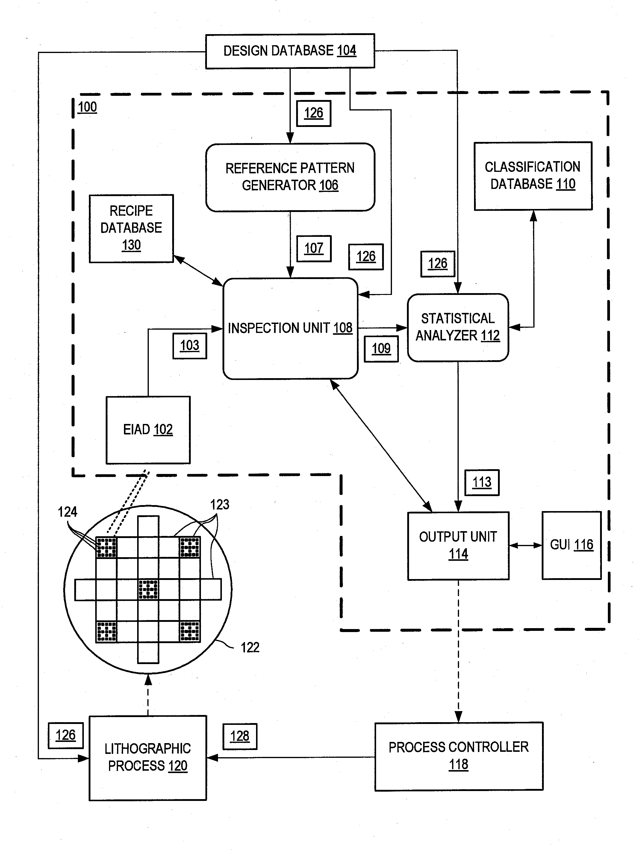
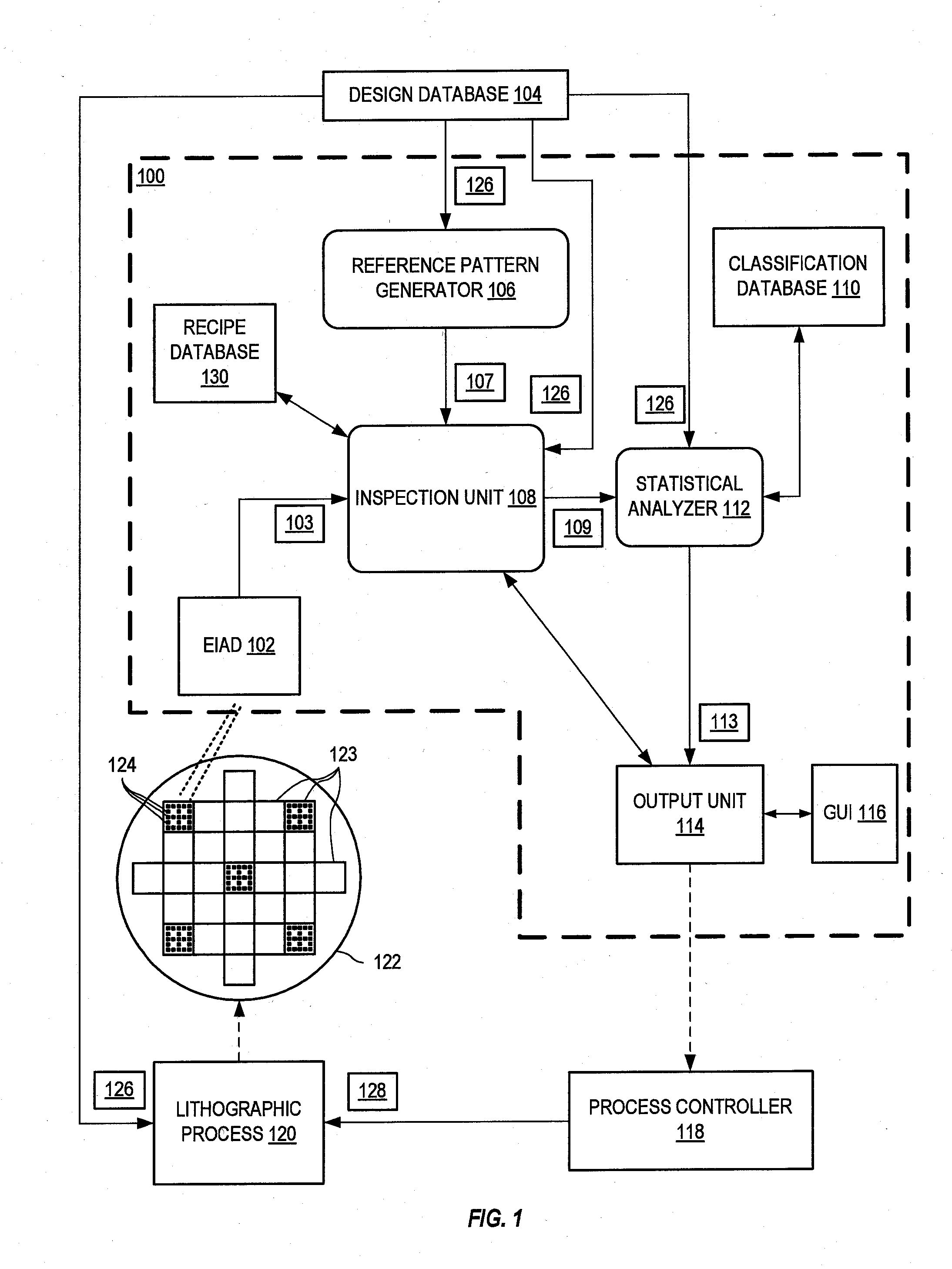
[0036]FIG. 1 shows one exemplary defect analysis system 100 for a semiconductor lithographic process 120. System 100 includes an electron image acquiring device (EIAD) 102, a reference pattern generator 106, an inspection unit 108, a statistical analyzer 112 and an output unit 114. System 100 may also include a graphical user interface (GUI) 116 that allows a user to interact with system 100 and view output from statistical analyzer 112. System 100 may include at least part of the functionality of the pattern inspection apparatus shown in FIG. 15 of U.S. application Ser. No. 11 / 987,766 (hereinafter the '766 Application), filed Dec. 4, 2007, incorporated herein by reference. For example, EIAD 102 may represent image generation device 7 shown in FIGS. 1, 15, 16, and 17 of the '766 Application; reference pattern generator 106 may represent reference pattern generation unit 11 shown in FIGS. 16 and 17 of the '766 Application; classification database 110 may represent defect class refere...


PUM


Abstract

Apparatus and method evaluate a wafer fabrication process for forming patterns on a wafer based upon design data. Within a recipe database, two or more inspection regions are defined on the wafer for analysis. Patterns within each of the inspection regions are automatically selected based upon tendency for measurement variation resulting from variation in the fabrication process. For each inspection region, at least one image of patterns within the inspection region is captured, a reference pattern, represented by one or both of (a) one or more line segments and (b) one or more curves, is automatically generated from the design data. An inspection unit detects edges within each of the images and registers the image with the reference pattern. One or more measurements are determined from the edges for each of the selected patterns and are processed within a statistical analyzer to form statistical information associated with the fabrication process.

Description

BACKGROUND[0001]Manufacture of semiconductor wafers uses a complex and precise lithographic process. Quality control and analysis of the lithographic process through each stage of wafer manufacture is critical to ensure the quality and reliability of the final product. Inconsistencies within the lithographic process are undesirable and early detection and correction of these inconsistencies saves a significant amount of time and expense for the manufacturer. For example, if problems with lithographic line and space definition can be identified after resist development and before etching, wafers can be reworked. Similarly, if lithographic issues can be identified soon after etching, process adjustments can be made many weeks sooner than would be required if wafer completion and electrical testing is required before making adjustments.[0002]Typically, wafers are viewed and measured using a critical dimension-scanning electron microscope (CD-SEM) technique, wherein an electron microsco...

Claims


Application Information

Patent Timeline
IPC IPC(8): G06K9/00
CPCG06T7/0006G06T2207/30148G06T7/0085G06T7/13
Inventor KITAMURA, TADASHIISHIKAWA, AKIO
Owner TASMIT INC
Why Eureka
Try Eureka