Low-cost flip-chip interconnect with an integrated wafer-applied photo-sensitive adhesive and metal-loaded epoxy paste system

a technology of photosensitive adhesive and flip-chip interconnect, which is applied in the direction of semiconductor devices, semiconductor/solid-state device details, electrical apparatus, etc., can solve the problems of reliability problems of conventional flip-chip interconnects, and achieve the effects of reducing the length of the manufacturing time, reducing the manufacturing cost of materials and equipment, and simplifying the process flow

Inactive Publication Date: 2010-06-24
TEXAS INSTR INC
View PDF4 Cites 11 Cited by
  • Summary
  • Abstract
  • Description
  • Claims
  • Application Information

AI Technical Summary

Benefits of technology

[0012]In this manner, the UV curable photo-sensitive adhesive can have an integrated function of conventional photo-resist and the underfill materials for flip-chip packaging technology. The printed conductive bumps can provide robust interconnects between the semiconductor dies and the base substrate.
[0013]Additionally, the new material systems and methods can simplify the process flow as compared with conventional packaging processes. Further, the length of the period of manufacturing time can be significantly reduced. Furthermore, manufacturing cost on mat...

Problems solved by technology

Due to such mechanical contacts, conventional...

Method used


Image

  • Low-cost flip-chip interconnect with an integrated wafer-applied photo-sensitive adhesive and metal-loaded epoxy paste system
  • Low-cost flip-chip interconnect with an integrated wafer-applied photo-sensitive adhesive and metal-loaded epoxy paste system
  • Low-cost flip-chip interconnect with an integrated wafer-applied photo-sensitive adhesive and metal-loaded epoxy paste system

Examples


Embodiment Construction

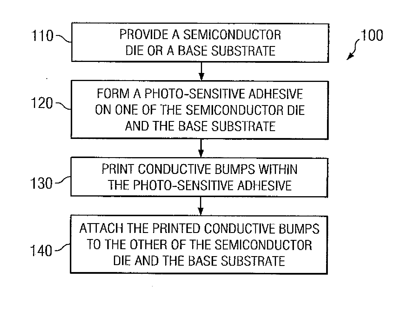
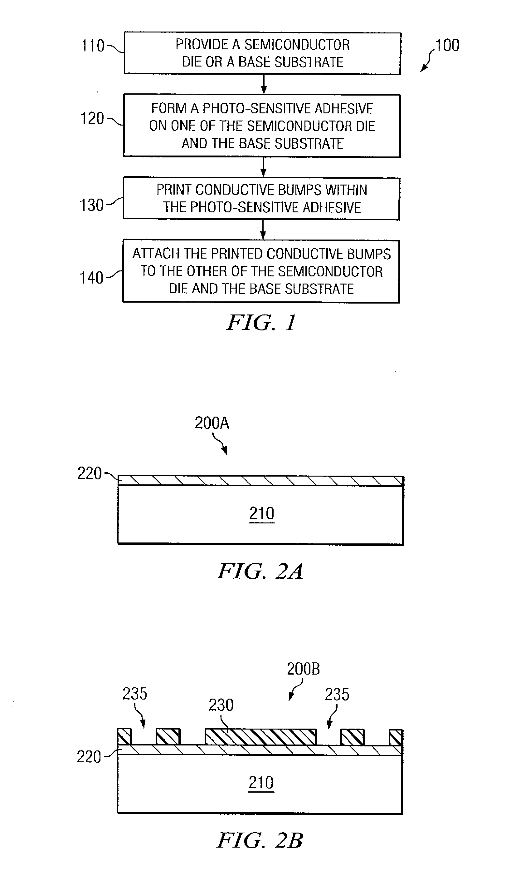
[0025]Various exemplary embodiments provide materials and methods for flip-chip packaging technology, which uses printed conductive bumps as flip-chip interconnects and is free of a combined use of the photo-resist and the underfill materials as used in the art. Reference will now be made in detail to exemplary embodiments of the invention, examples of which are illustrated in the accompanying drawings. Wherever possible, the same reference numbers will be used throughout the drawings to refer to the same or like parts.

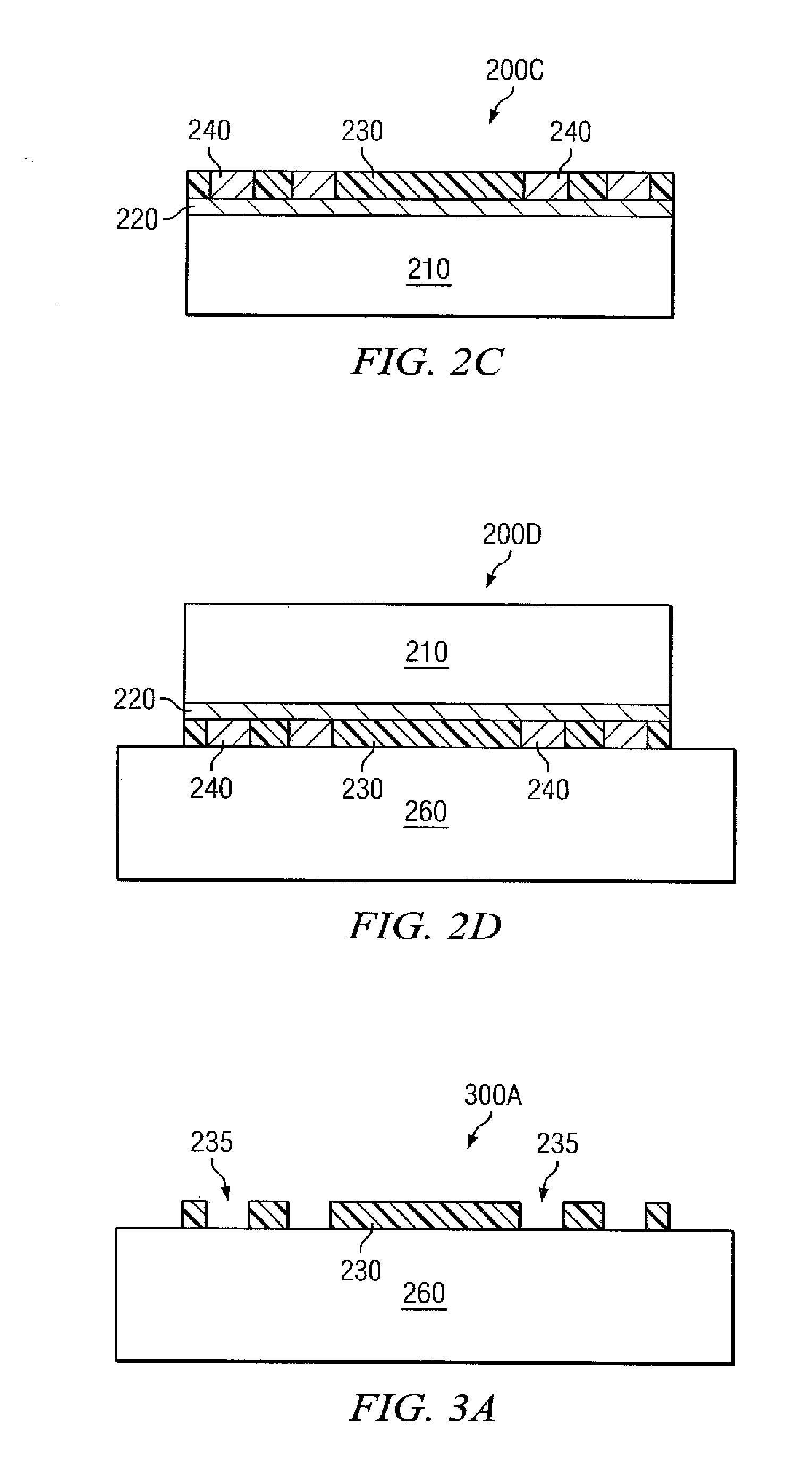
[0026]In embodiments, the disclosed flip-chip packaging technology can use a photo-sensitive adhesive that includes curable polymeric precursors. In one embodiment, a photo-sensitive adhesive can be applied on a semiconductor die and / or a base substrate with conductive bumps formed, e.g., printed, in through-openings of the photo-sensitive adhesive. One or more semiconductor dies or a semiconductor wafer with a plurality of semiconductor dies can then be laterally pac...


PUM


Abstract

Various exemplary embodiments provide materials and methods for flip-chip packaging technology. The disclosed flip-chip packaging technology can use a single B-stage wafer-applied photo-sensitive adhesive along with printed interconnects, which does not include conventional underfill materials and processes. In one embodiment, a photo-sensitive adhesive can be applied on a semiconductor die or a base substrate with conductive bumps printed in through-openings of the photo-sensitive adhesive. One or more semiconductor dies can be laterally packaged or vertically stacked on the base substrate using the printed conductive bumps as interconnects there-between.

Description

RELATED APPLICATIONS[0001]This application claims priority from U.S. Provisional Patent Applications Ser. No. 61 / 139,393, filed Dec. 19, 2008, which is hereby incorporated by reference in its entirety.FIELD OF THE INVENTION[0002]The invention relates generally to semiconductor device assembly and packaging and, more specifically, to flip-chip packaging of integrated circuit (IC) devices.BACKGROUND OF THE INVENTION[0003]In flip-chip packaging processes, when plated metal bumps are used, a photo-resist is first applied on a wafer or semiconductor die. Then, it is exposed and developed to create openings at the bump locations. Subsequently, a conductive material is plated into the passivation openings in the photo-resist to create metal bumps. The conductive material is typically solder, copper, copper plus solder or solder-loaded epoxy paste.[0004]After the flip-chip metal bumps are created, the semiconductor die is attached to the substrate. Due to the presence of the bumps on the se...

Claims


Application Information

Patent Timeline
IPC IPC(8): H01L21/78H01L21/60
CPCH01L21/563H01L23/295H01L24/11H01L24/13H01L24/27H01L24/29H01L24/32H01L24/73H01L24/91H01L24/94H01L2224/11318H01L2224/1132H01L2224/1148H01L2224/11515H01L2224/13099H01L2224/13109H01L2224/13111H01L2224/13116H01L2224/13139H01L2224/13144H01L2224/13147H01L2224/13155H01L2224/1329H01L2224/13339H01L2224/13347H01L2224/27318H01L2224/2732H01L2224/274H01L2224/27416H01L2224/27436H01L2224/27438H01L2224/27515H01L2224/27602H01L2224/29011H01L2224/2919H01L2224/2929H01L2224/29387H01L2224/29388H01L2224/73104H01L2224/73203H01L2224/81801H01L2224/8185H01L2224/83191H01L2224/83856H01L2224/921H01L2224/94H01L2224/95H01L2924/01005H01L2924/01029H01L2924/01047H01L2924/0105H01L2924/01079H01L2924/01082H01L2924/09701H01L2924/14H01L2924/01006H01L2924/01033H01L2924/014H01L2924/0665H01L2224/29101H01L2224/73204H01L2224/81191H01L2224/81192H01L2224/83192H01L2924/1461H01L2924/00H01L2924/15787H01L2224/27618H01L2224/05548H01L2224/05573H01L2924/00014H01L2224/0554H01L2224/05599H01L2224/0555H01L2224/0556
Inventor DUNNE, RAJIV CARLCOWENS, MARVIN WAYNEBOLANOS, MARIO ANTONIO
Owner TEXAS INSTR INC
Why Eureka
Try Eureka