Light emitting diode

a diode and light-emitting technology, applied in the direction of basic electric elements, electrical equipment, semiconductor devices, etc., can solve the problems of reducing reducing the efficiency of devices, so as to increase the overall perimeter of vertical layer structure, enhance light extraction, and uniform current density

Inactive Publication Date: 2010-07-01
OPTOGAN OY
View PDF10 Cites 13 Cited by
  • Summary
  • Abstract
  • Description
  • Claims
  • Application Information

AI Technical Summary

Benefits of technology

[0008]According to the present invention, a vertical trench is formed between the electrodes, the trench extending through the chip, including the lower current-distributing layer, for controlling the horizontal current flow in the current-distributing layers in order to achieve a uniform current density over the active layer. In other words, in contrast to the prior art solutions where the current flow is controlled by the geometries of the electrodes and the vertical layer structure above the lower current-distributing layer only, in the present invention also the lower current distribution is selectively cut off. Thus, instead of the two-level approach of the prior art solutions, the chip topology is based on three levels. By controlling the current flow by excluding all layers from selected sites of the chip geometry, a unidirectional current flow and a very uniform current density over the entire light-generating layer can be achieved.
[0009]In addition to the current guiding effect, trenches described above increase the overall perimeter of the vertical layer structure. This produces an increased probability for light generated in the active layer to escape from the structure through the side walls of the vertical layer structure. For further enhancing the light extraction from the chip, in a preferred embodiment of the present invention an additional vertical trench is formed between the electrodes, the additional trench extending through the chip, including the active layer, along the horizontal direction of current flow in the current-distributing layers for further increasing the overall perimeter of the vertical layer structure. Additional trenches positioned along the current flow direction do not disturb the current flow.

Problems solved by technology

However, in most practical cases, said sheet resistances produce substantial voltage drops along the current-distributing layers.
This leads to a non-uniform current density resulting possibly in local overheating at the high current density sites.
This local overheating can further result in a drop in the device efficiency, as well as in degraded device reliability.
The problem is that, in most practical cases, the horizontal chip dimensions are clearly higher than the current spreading length.
Thus, with conventional simple contact pads, said condition relating to the distance between the electrodes can not be fulfilled.
However, also this approach has its deficiencies: current density is always highest near the electrodes, particularly at the outer ends of the electrode “fingers”, resulting in a significantly non-uniform current density.

Method used


Image

  • Light emitting diode
  • Light emitting diode
  • Light emitting diode

Examples


Embodiment Construction

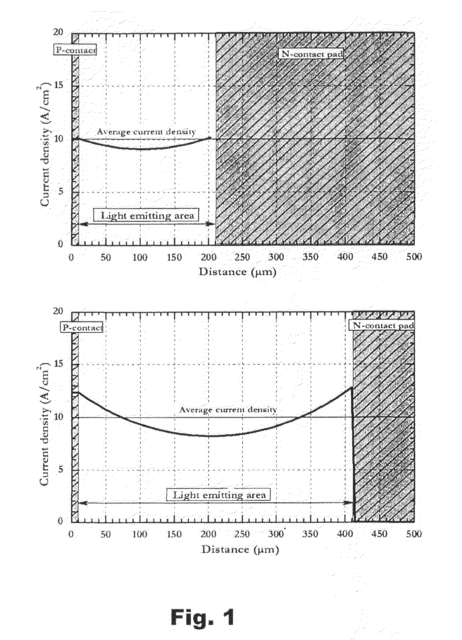
[0016]FIG. 1 shows calculated current densities in a linear LED chip with a length of (the upper graph) 200 μm and (the lower graph) 400 μm. The current spreading length in both cases is 200 μm. As is seen in the figure, due to the large horizontal dimensions relative to the current spreading length, current density in both cases is not uniform, uniformity becoming higher with increase of the chip length. One can see that in the second case, current density is far from uniform.

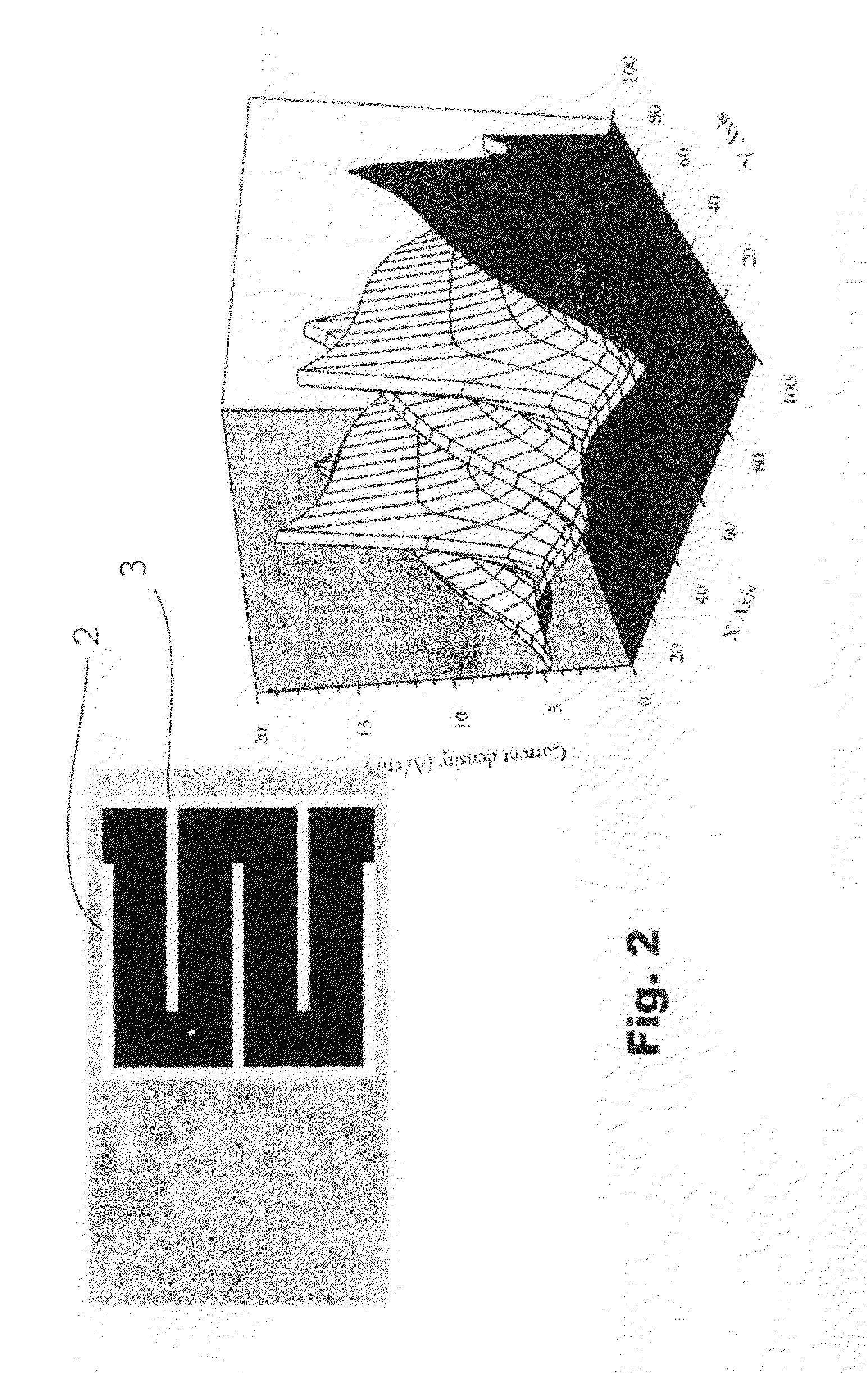
[0017]The interdigitated electrodes 2, 3 of the LED design of FIG. 2 are arranged to provide a distance between the electrodes smaller than the current spreading length. In spite of this, as is seen in the graph of FIG. 2, the current density over the chip area is highly non-uniform having very strong local maxima at the ends of the finger-like protrusions of the electrodes.

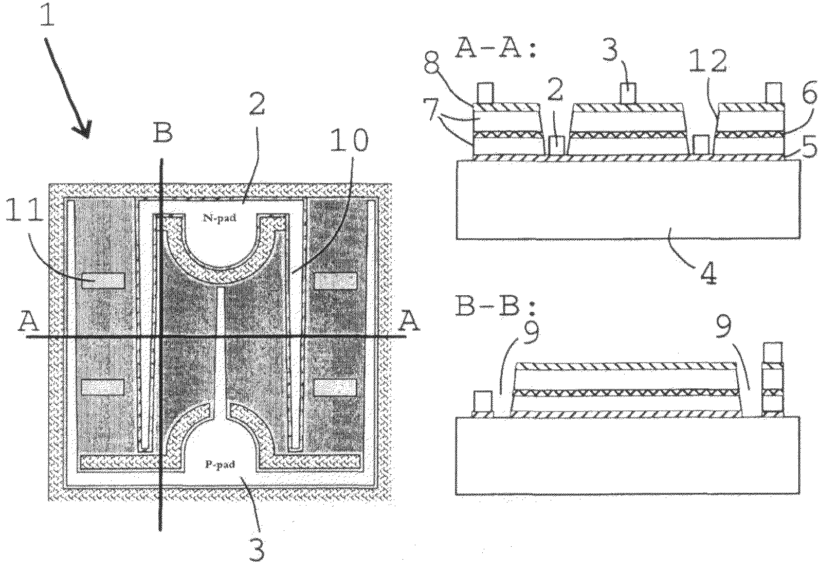
[0018]In the LED chip 1 of FIG. 3, the first and second electrodes 2, 3 establish a modified interdigitated geometry extending over the en...


PUM


Abstract

An LED chip (1) grown on an electrically insulating substrate (4) comprises a lower current-distributing layer (5) of a first conductivity type, a first electrode (2), a vertical layer structure (5, 6, 7), the last two being formed on the lower current-distributing layer horizontally separated from each other, the vertical layer structure comprising an active layer (6) and an upper current-distributing layer (8) of a second conductivity type above the active layer, and a second electrode (3) formed on the upper current-distributing layer, the geometry of the electrodes being adjusted to provide a horizontal distance between the electrodes lower than the current spreading length of the chip. According to the present invention, a vertical trench (9) is formed between the electrodes (2, 3), the trench extending through the chip (1), including the lower current-distributing layer (5), for controlling the horizontal current flow in order to achieve a uniform current density over the active layer (6).

Description

FIELD OF THE INVENTION[0001]The present invention relates to a light-emitting diode (LED) chip design, the LED being grown on an insulating substrate.BACKGROUND OF THE INVENTION[0002]In an LED grown as a layer structure on an insulating substrate, both n- and p-contact electrodes are made from the top side of the chip. Normally they are located near the opposite edges of the light-generating region of the chip. One of them is formed on a lower current-distributing layer exposed by selectively etching away the layers grown on it and the other on an upper current-distributing layer on top of the LED layer structure.[0003]In a typical case, the horizontal distance between the electrodes is much higher than the overall thickness of the vertical layer structure of the LED. In that case, to provide a high current uniformity over the light-generating layer, the sheet resistances of the current-distributing layers should be as low as possible in order to minimize voltage drop along those la...

Claims


Application Information

Patent Timeline
Patent Type & Authority Applications(United States)
IPC IPC(8): H01L33/00H01L33/20H01L33/38
CPCH01L33/20H01L33/38
Inventor BOUGROV, VLADISLAV E.ODNOBLVUDOV, MAXIM A.
Owner OPTOGAN OY
Why Eureka
Try Eureka