Reducing High-Frequency Signal Loss in Substrates

Active Publication Date: 2010-07-01
TAIWAN SEMICON MFG CO LTD
View PDF9 Cites 6 Cited by
  • Summary
  • Abstract
  • Description
  • Claims
  • Application Information

AI Technical Summary

Benefits of technology

[0007]The advantageous features of the embodiments include reduced signal loss for high-frequency devices. In addition, the em

Problems solved by technology

A common problem faced by designers is the signal loss in the substrates that are underlying the high-frequency circuits, which signal loss is partially caused by the parasitic capacitors formed between the high-frequency circuits and the underlying substrates.
Typically, with the increase in the frequency of the signals, the loss also increases.
This significantly limits the design of high-frequency circuits.
The signal loss also occurs to other integrated circuit

Method used


Image

  • Reducing High-Frequency Signal Loss in Substrates
  • Reducing High-Frequency Signal Loss in Substrates
  • Reducing High-Frequency Signal Loss in Substrates

Examples


Example

[0014]The making and using of the embodiments are discussed in detail below. It should be appreciated, however, that the embodiments provide many applicable inventive concepts that can be embodied in a wide variety of specific contexts. The specific embodiments discussed are merely illustrative of specific ways to make and use the invention and do not limit the scope of the invention.

[0015]A novel substrate-loss reduction structure and the method of forming the same are presented. The intermediate stages of manufacturing embodiments of the present invention are discussed. The variations of the embodiments are also discussed. Throughout the various views and illustrative embodiments of the present invention, like reference numbers are used to designate like elements.

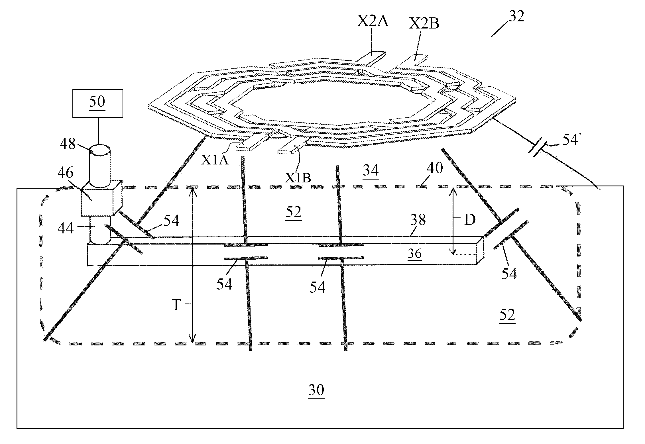
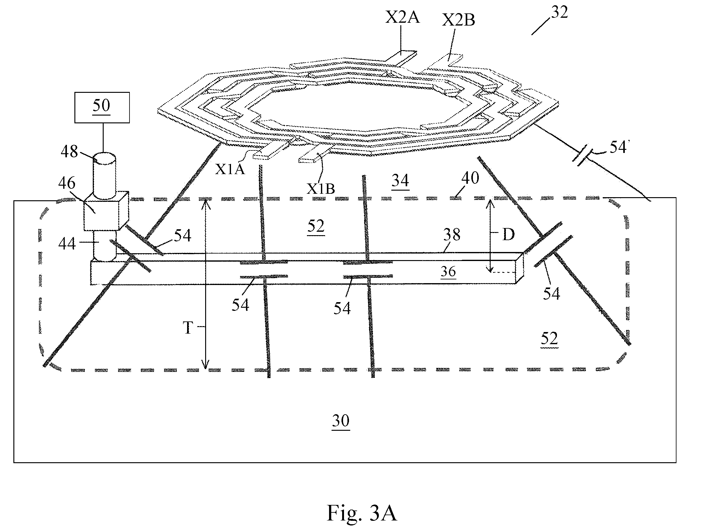
[0016]FIG. 3A illustrates a perspective view of an embodiment of the present invention, which includes substrate 30. Substrate 30 may be a semiconductor substrate comprising silicon, germanium, GaAs, and / or other commonly...


PUM


Abstract

An integrated circuit structure includes a semiconductor substrate of a first conductivity type; and a depletion region in the semiconductor substrate. A deep well region is substantially enclosed by the depletion region, wherein the deep well region is of a second conductivity type opposite the first conductivity type. The depletion region includes a first portion directly over the deep well region and a second portion directly under the deep well region. An integrated circuit device is directly over the depletion region.

Description

TECHNICAL FIELD[0001]This invention relates generally to integrated circuits, and more particularly to high-frequency integrated circuit devices, and even more particularly to the structures for reducing signal loss in substrates and methods for forming the same.BACKGROUND[0002]High-frequency circuits are commonly used in modern applications such as wireless communication applications. A common problem faced by designers is the signal loss in the substrates that are underlying the high-frequency circuits, which signal loss is partially caused by the parasitic capacitors formed between the high-frequency circuits and the underlying substrates. Typically, with the increase in the frequency of the signals, the loss also increases. This significantly limits the design of high-frequency circuits.[0003]FIG. 1 illustrates conventional radio frequency (RF) transformer 4 formed over semiconductor substrate 2. Dielectric layer(s) 8 separates RF transformer 4 from semiconductor substrate 2. RF...

Claims


Application Information

Patent Timeline
IPC IPC(8): H01L29/06
CPCH01L23/5227H01L23/645H01L27/08H01L2924/0002H01L2924/00
Inventor JOU, CHEWN-PUCHEN, HO-HSIANG
Owner TAIWAN SEMICON MFG CO LTD
Why Eureka
Try Eureka