Circuit Board Structure of Integrated Optoelectronic Component

Active Publication Date: 2007-04-19
PHOENIX PRECISION TECH CORP
View PDF4 Cites 27 Cited by
  • Summary
  • Abstract
  • Description
  • Claims
  • Application Information

AI Technical Summary

Benefits of technology

[0025] In addition, a heat slug can be formed in the supporting structure or the second supporting board described before, so as to connect to the optical transceiver or the semiconductor component, so that the heat generated from running the optical transceiver or the semiconductor component can be directly dispelled outwards. As a result, the heat dissipation efficiency of the circuit boa

Problems solved by technology

The most straightforward method for raising the processing speed of semiconductors is to increase its operating frequency, but when the data transfer rate exceeds one gigabyte per second problems like heat dissipation caused by high wattage, signal time delay and electromagnetic interference (EMI) also arise, which will impede the production of semiconductors with high performance.
This problem has been made even more severe because the traditional medium for data signal transmission is copper circuit, which cannot achieve higher conductivity due to its intrinsically limited conducting property, thus its signal transmission rate cannot be elevated by the method of increasing its conductivity.
Moreover, the signal transmission structure made of metal circuits is more susceptible to the interference of external noises or internal circuits during signal transmission, which in turn leads to erroneous signals being transferred.
The protective measures will result in increased difficulty to the d

Method used


Image

  • Circuit Board Structure of Integrated Optoelectronic Component
  • Circuit Board Structure of Integrated Optoelectronic Component
  • Circuit Board Structure of Integrated Optoelectronic Component

Examples


first embodiment

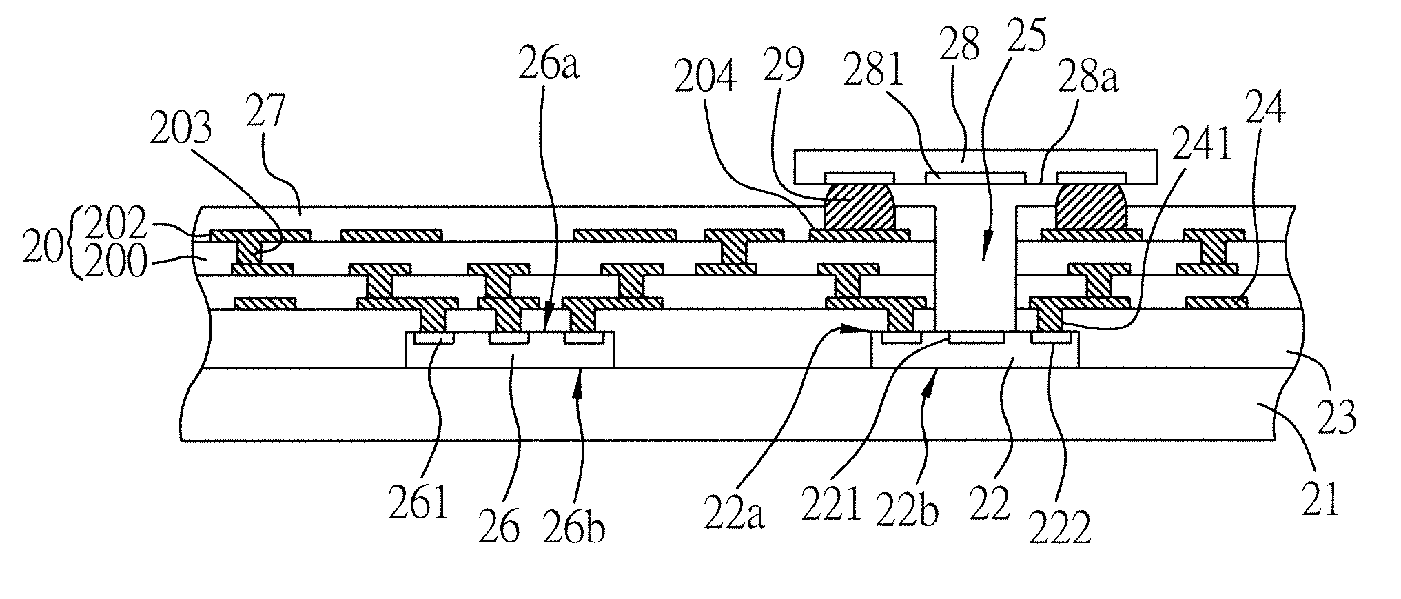
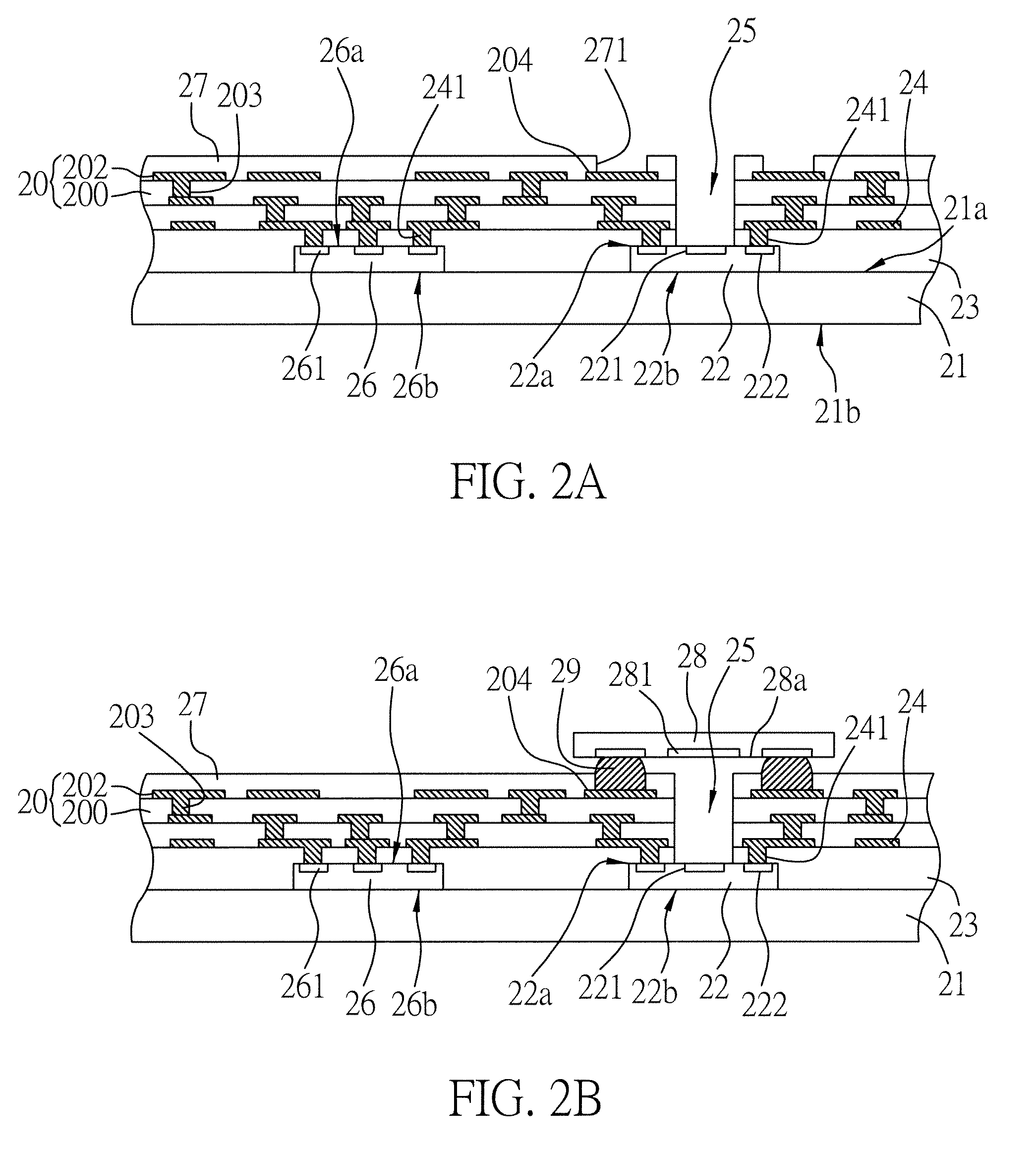
[0036]FIGS. 2A and 2B show the cross-sectional views of the circuit board structure of integrated optoelectronic component of the present invention according to the present invention.

[0037] As shown in FIG. 2A, the circuit board structure of integrated optoelectronic component in this embodiment is composed of a supporting structure 21 that has a first surface 21a and a second surface 21b opposite to the first surface; an optical transceiver 22 that has at least one active surface 22a and an inactive surface 22b opposite to 22a; the inactive surface 22b of optical transceiver 22 is disposed on the first surface 21a of supporting structure 21, an optical active region 221 and a plurality of electrode pads 222 are formed on active surface 22a of optical transceiver 22; a dielectric layer 23 that is formed on the first surface 21a of supporting structure 21 and on active surface 22a of optical transceiver 22; a circuit layer 24 that is formed on the surface of dielectric layer 23, and ...

second embodiment

[0046]FIG. 3 is a cross-sectional view showing the circuit board structure of integrated optoelectronic component of the present invention according to the present invention; it differs from the previous embodiment in that the supporting structure 31 can be either a circuit board or an insulating board, and an opening 310 is formed in supporting structure 31, with a heat slug 312 formed in opening 310. The optical transceivers 22 and 28, as well as semiconductor component 26 are disposed on heat slug 312, so that the heat generated from running optical transceivers 22 and 28 or semiconductor component 26 can be dispelled outwards, thereby raising the heat dissipation function of the circuit board structure of integrated optoelectronic component and protecting the components from getting damaged.

The Third Preferred Embodiment

third embodiment

[0047]FIGS. 4A and 4B are schematic cross-sectional views illustrating the circuit board structure of integrated optoelectronic component of the present invention according to the present invention.

[0048] As shown in FIG. 4A, the circuit board structure of integrated optoelectronic component in this embodiment is composed of: a supporting structure 41 that has a first surface 41a and a second surface 41b, the supporting structure 41 can either be metal boards, ceramic boards, insulating boards, organic circuit boards, or the randomly stacked structure made of the previous materials, an opening 410 that penetrates the first surface 41a but not the second surface 41b is formed in supporting structure 41; at least one optical transceiver 22 that has an active surface 22a and an inactive surface 22b opposite to 22a, and the inactive surface 22b of optical transceiver 22 is disposed in opening 410 of supporting structure 41 by an adhesive layer (not shown in the figure); at least a semic...


PUM


Abstract

A circuit board structure of an optoelectronic component is proposed. A supporting structure has a first surface and a second surface. At least one optical transceiver has an active surface and an inactive surface. The inactive surface of the optical transceiver is mounted on the first surface of the supporting structure, and the active surface of the optical transceiver has an optical active region and a plurality of electrode pads. A dielectric layer is formed on the first surface of the supporting structure and the active surface of the optical transceiver. A circuit layer is formed on the dielectric layer and is electrically connected to the electrode pads on the active surface of the optical transceiver through the conductive structure in the dielectric layer. At least one hole, which penetrates the dielectric layer, is used to expose the optical active region on the active surface of the optical transceiver. Therefore, the transmission quality of the optical transceiver is improved and the dimension of the circuit board structure is shrunken.

Description

FIELD OF THE INVENTION [0001] The present invention is related to circuit board structures of integrated optoelectronic component, and more particularly, to a circuit board structure that has been integrated with optical transmitting and receiving components and circuit structures. BACKGROUND OF THE INVENTION [0002] As the technological development of semiconductors advances, demands for miniaturized packaging and larger data storage capacity have also intensified along the way. In addition to that, because the data processing capacity is constantly increasing, if data units of the same size can be processed at the fastest speed possible in a given unit of time, then data can be processed more efficiently. The most straightforward method for raising the processing speed of semiconductors is to increase its operating frequency, but when the data transfer rate exceeds one gigabyte per second problems like heat dissipation caused by high wattage, signal time delay and electromagnetic i...

Claims


Application Information

Patent Timeline
IPC IPC(8): G02B6/12
CPCG02B6/43H01L23/48H01L24/16H01L25/167H01L2224/13099H01L2224/16237H01L2224/24227H01L2224/32188H01L2924/01002H01L2924/01029H01L2924/01046H01L2924/15153H01L2924/15165H01L2924/1517H05K1/0274H05K1/181H05K1/185H05K2201/09072H01L2924/01033H01L2924/014H01L2924/12041H01L2924/12043H01L2224/05571H01L2224/05573H01L2924/00014H01L2924/00H01L2224/05599
Inventor HSU, SHIH-PING
Owner PHOENIX PRECISION TECH CORP
Why Eureka
Try Eureka