Semiconductor device and semiconductor package including the same

a semiconductor and semiconductor technology, applied in the direction of stacked capacitors, fixed capacitor details, thin/thick film capacitors, etc., can solve the problems of increasing the amount of power ground grid noise and power ground grid noise in semiconductor devices, and achieve the effect of reducing the noise of power ground grid

Active Publication Date: 2010-07-01
SK HYNIX INC
View PDF6 Cites 20 Cited by
  • Summary
  • Abstract
  • Description
  • Claims
  • Application Information

AI Technical Summary

Benefits of technology

[0012]According to the present invention, much capacitance of the decoupling capacitor can be endured by providing the decoupling capacitor formed on a separate semiconductor chip without increasing the area thereof, thereby removing efficiently the power ground grid noise.
[0013]Additionally, according to the present invention, a decoupling capacitance of the decoupling capacitor can be endured easily by providing the decoupling

Problems solved by technology

A power ground grid noise may occur in a semiconductor device, when current is consumed abruptly and a plurality of signals are inputted/outputted si

Method used


Image

  • Semiconductor device and semiconductor package including the same
  • Semiconductor device and semiconductor package including the same
  • Semiconductor device and semiconductor package including the same

Examples


Embodiment Construction

[0020]Other objects and advantages of the present invention can be understood by the following description, and become apparent with reference to the embodiments of the present invention. In the figures, the dimensions of layers and regions may be exaggerated for clarity of illustration. Like reference numerals refer to like elements throughout.

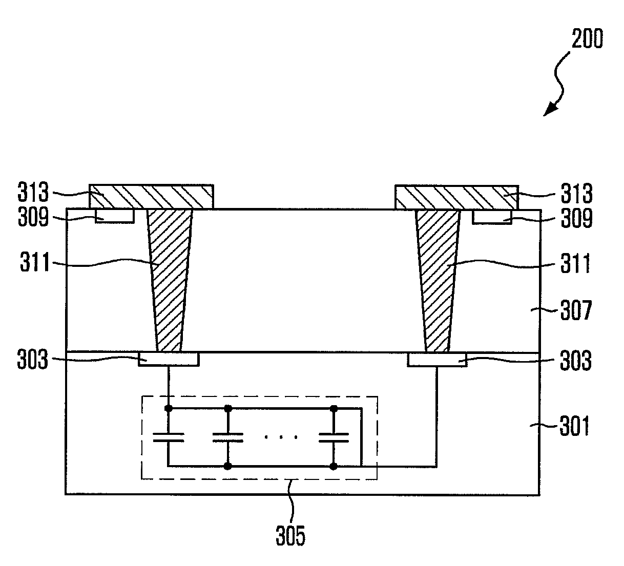
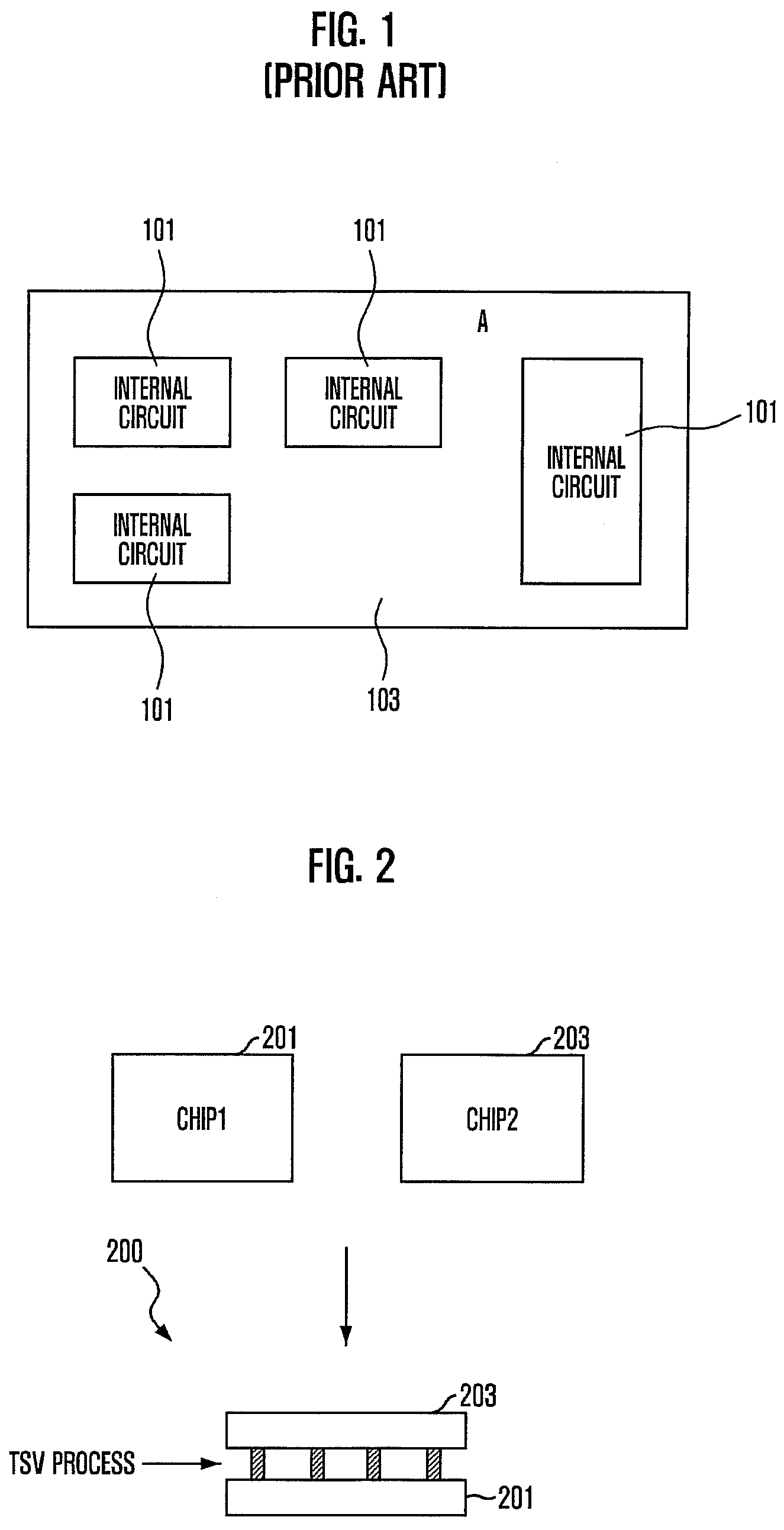
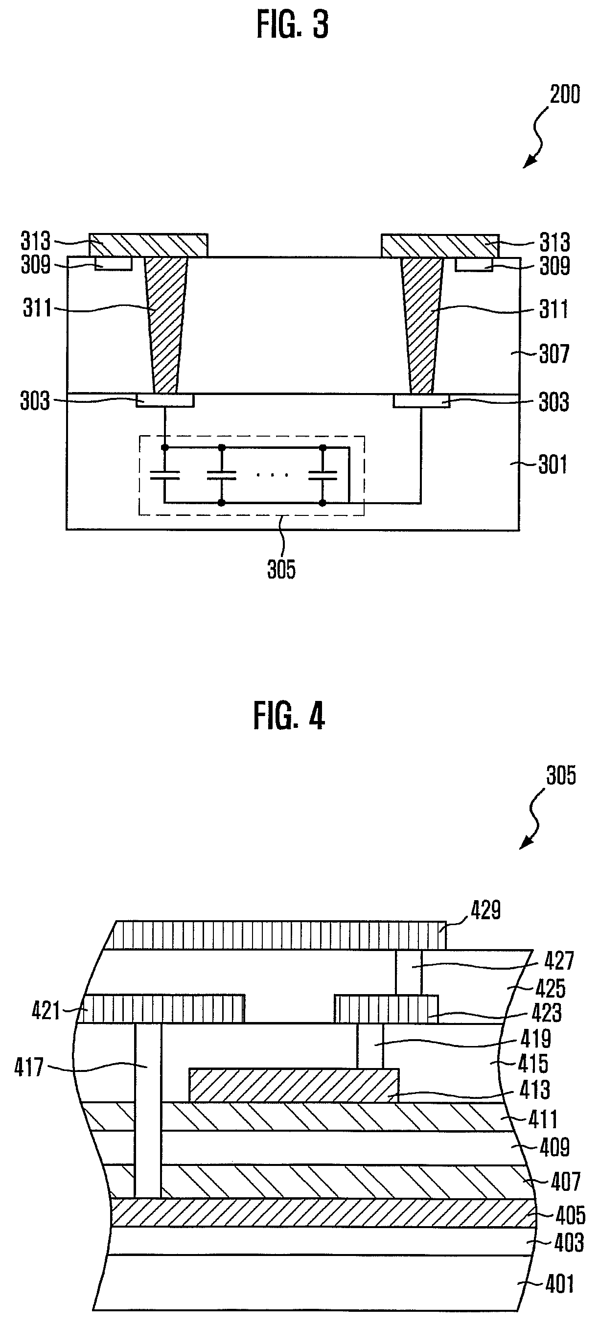
[0021]FIG. 2 a view illustrating a semiconductor device 200 according to an embodiment of the present invention.

[0022]Referring FIG. 2, the semiconductor device 200 includes a first semiconductor chip 201 and a second semiconductor chip 203. The second semiconductor chip 203 is stacked over the first semiconductor chip 201.

[0023]The first semiconductor chip 201 includes at least one capacitor. The second semiconductor chip 203 includes internal circuits for processing inputted signals. The capacitor of the first semiconductor chip 201 may be a decoupling capacitor for removing the power ground rid noise.

[0024]Differently from the conventional...


PUM


Abstract

Provided is a semiconductor device capable of removing a power ground grid noise using a small area. The semiconductor device includes a first chip including at least one decoupling capacitor; and a second semiconductor chip stacked over the first semiconductor chip, including internal circuits.

Description

CROSS-REFERENCE TO RELATED APPLICATIONS[0001]The present invention claims priority of Korean patent application number 10-2008-0134579, filed on Dec. 26, 2008, which is incorporated by reference in its entirety.BACKGROUND OF THE INVENTION[0002]The present invention relates to a semiconductor device and a semiconductor package, and more particularly, to a semiconductor device and a semiconductor package having the same, including a decoupling capacitor.[0003]A power ground grid noise may occur in a semiconductor device, when current is consumed abruptly and a plurality of signals are inputted / outputted simultaneously. As an integration degree and an operation speed of the semiconductor device increase, an amount of the power ground grid noise increases. Typically, a decoupling capacitor has been used to remove the power ground grid noise. The decoupling capacitor connects between a region for providing a power voltage (VDD) and a region for providing a ground voltage (VSS) and acts a...

Claims


Application Information

Patent Timeline
IPC IPC(8): H01L23/06H01L23/52H01G4/228H01L25/16
CPCH01G4/232H01G4/30H01L2924/00014H01L2224/056H01L2224/05568H01G4/33H01G4/40H01L23/3128H01L23/481H01L23/5223H01L23/642H01L25/0657H01L2225/06513H01L2225/06517H01L2225/06527H01L2225/06541H01L2924/15311H01L2924/19104H01L2224/16146H01L2224/05001H01L2224/05009H01L2224/0557H01L2224/05099H01L2224/08146H01L24/05H01L27/04H01L23/52
Inventor LEE, JUN-HOLEE, HYUNG-DONGKIM, HYUN-SEOK
Owner SK HYNIX INC
Why Eureka
Try Eureka