Non-volatile one-time - programmable and multiple-time programmable memory configuration circuit

a configuration circuit and non-volatile technology, applied in the direction of instruments, computation using denominational number representation, pulse technique, etc., can solve the problems of inability to optimize the device, the inability to programmable and mtp memory still incorporating otp and mtp memories, and the cost of additional processing steps, etc. problem, to achieve the effect of self-limiting the amount of energy consumption during programming

Inactive Publication Date: 2010-07-01
INVENSAS CORP
View PDF50 Cites 11 Cited by
  • Summary
  • Abstract
  • Description
  • Claims
  • Application Information

AI Technical Summary

Problems solved by technology

These devices, however, are not optimal, however, as they require additional processing step to embed them within a logic circuit.
Incorporating OTP and MTP memories nonetheless also typically comes at the expense of some additional processing steps.
In addition, since an NMOS device's programming mechanism with channel hot electrons injection is self-limiting, unlike that case of a PMOS with channel hot electron programming, the amount of energy consumption during programming is self-limited for this invention.
However, it is unclear whether the device actually works in the way the inventors claim.
That is, it is not apparent that the channel current will be initiated to induce hot-hole-injection since the state of the floating gate is unknown and there is no available means to couple a voltage unto the floating gate.
This is not a very optimal behavior for a memory device.
The drawbacks of this cell, however, include the fact that the cell and channel 412 must be asymmetric, and the coupling is only controlled using the length dimension of the active regions.
Because of these limitations, it also does not appear to be extendable to a multi-level architecture.
Moreover, it apparently is only implemented as a p-channel device.

Method used


Image

  • Non-volatile one-time - programmable and multiple-time programmable memory configuration circuit
  • Non-volatile one-time - programmable and multiple-time programmable memory configuration circuit
  • Non-volatile one-time - programmable and multiple-time programmable memory configuration circuit

Examples


Embodiment Construction

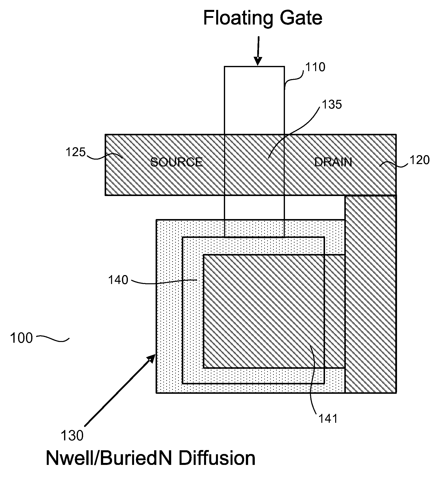
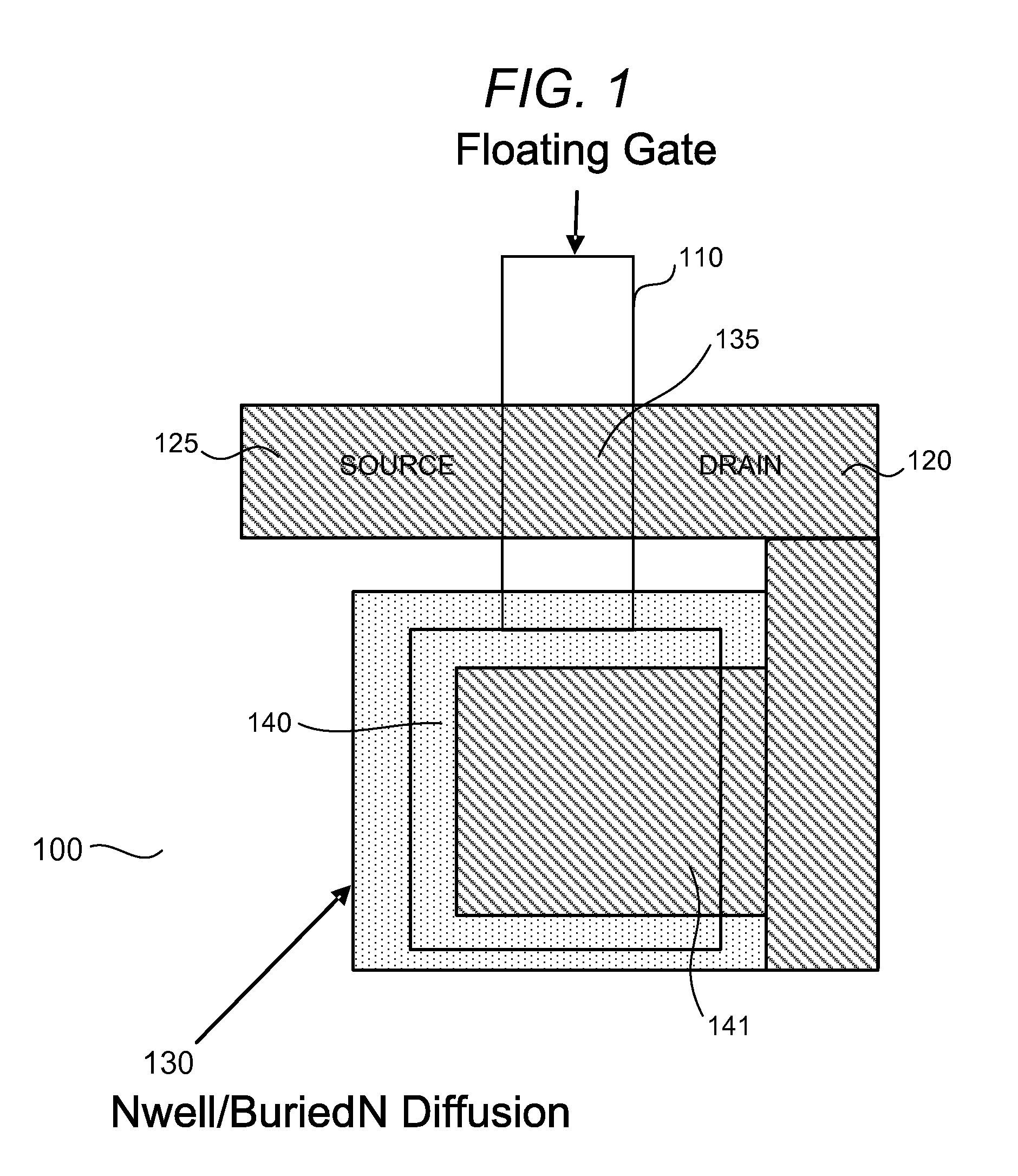
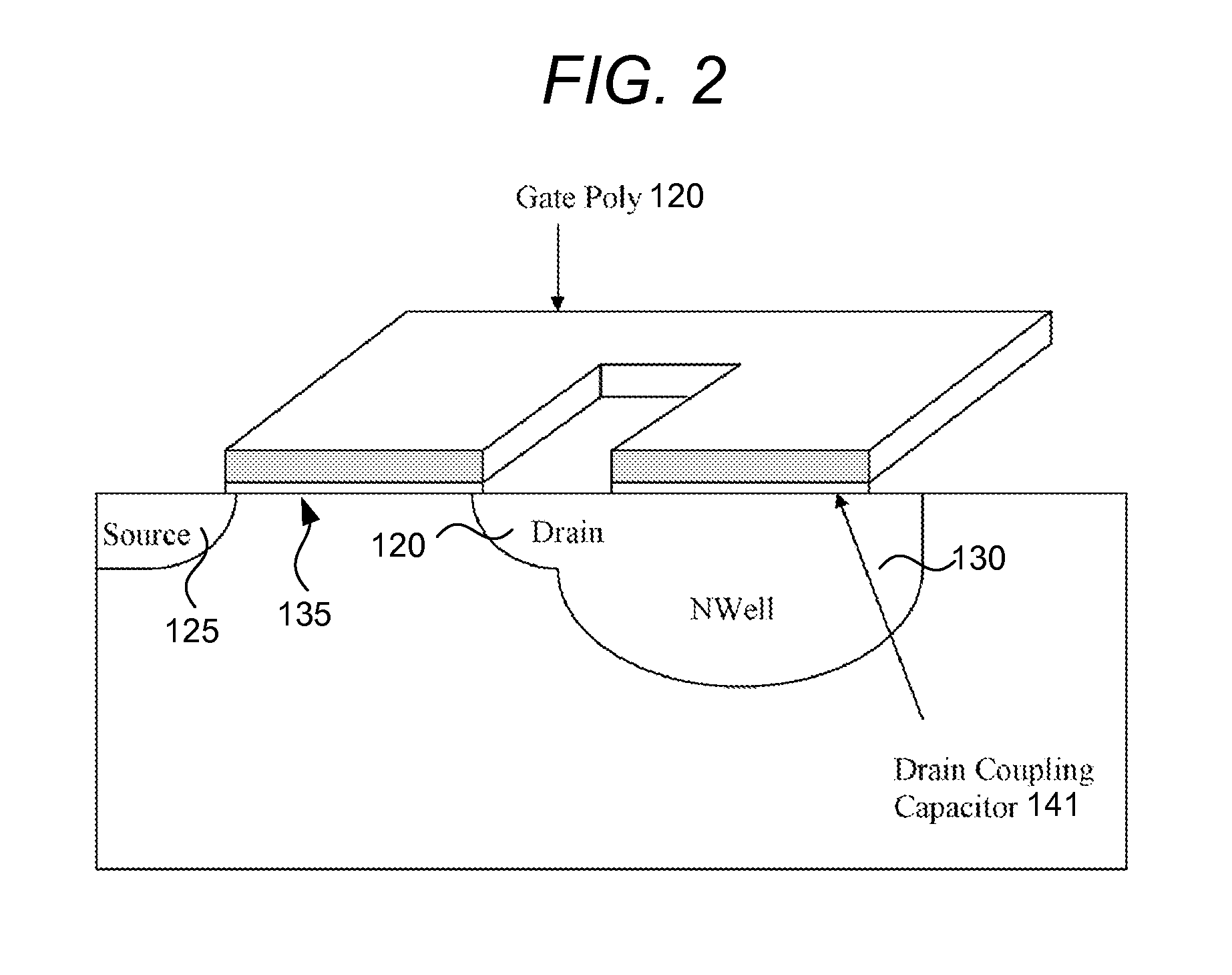
[0021]The present disclosure concerns a new type of non-volatile configuration circuit (preferably single poly) that can be operated either as an OTP (one time programmable) or as an MTP (multiple time programmable) memory cell. The preferred device structure is fully compatible with advanced CMOS logic process, and would require, at the worst case, very minimal additional steps to implement.

[0022]A unique aspect of the present device is that the floating gate of the memory cell structure is electrically coupled strongly through a variable number of S / D junctions of the transistor, whereas traditional single poly nonvolatile memory cells require either an additional interconnect layer to couple to the floating gate, or the floating gate has virtually none or minimal electrical coupling to any of the existing electrical signals. Moreover, unlike the 2008 / 0186772 reference, the coupling ratio can be more specific and precise. That is, by exactly controlling the coupling ratio (through...


PUM


Abstract

A programmable non-volatile configuration circuit uses a pair of non-volatile memory devices arranged in a pull-up and pull-down arrangement. The non-volatile memory devices have floating gates that overlaps a variable portion of a source/drain region. This allows a programming voltage for the device to be imparted to the floating gate through variable capacitive coupling, thus changing the state of the device. The invention can be used in environments to store configuration data for programmable logic devices, field programmable arrays, and many other applications.

Description

RELATED APPLICATION DATA[0001]The present application claims the benefit under 35 U.S.C. 119(e) of the priority date of Provisional Application Ser. No. 61 / 141,618 filed Dec. 30, 2008 which is hereby incorporated by reference. The application is further related to Ser. Nos. 12 / 264,029, 12 / 264,060 and 12 / 264,076 all filed Nov. 3, 2008 which are hereby incorporated by reference.FIELD OF THE INVENTION[0002]The present invention relates to non-volatile configuration circuits which can be programmed one time, or multiple times in some instances. The invention has particular applicability to applications where is it desirable to customize electronic circuits, including programmable logic devices, field programmable gate arrays, etc.BACKGROUND[0003]Field Programmable Gate Arrays (FPGAs) are well-known circuits used in a variety of electronic devices / computing systems. FPGAs offer the ability to update their functionality in the field, which is a substantial advantage over fixed ASIC type d...

Claims


Application Information

Patent Timeline
Patent Type & Authority Applications(United States)
IPC IPC(8): G11C17/00H03K19/177
CPCG11C16/0441G11C17/14G11C2216/10G11C2216/26H03K19/0002H01L27/11558H01L27/11803H01L29/7885H03K19/177H01L27/11521H10B41/60H10B41/30
Inventor LIU, DAVID K.Y.
Owner INVENSAS CORP
Why Eureka
Try Eureka