

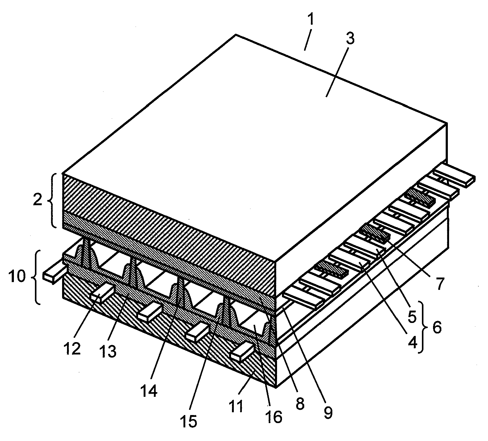
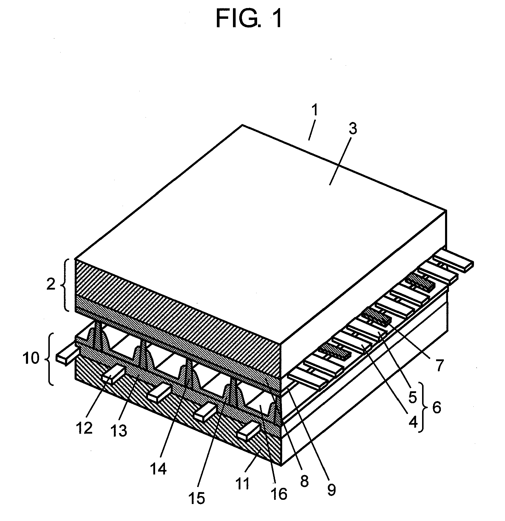
Plasma display panel and method for manufacturing the same
a technology of display panel and plasma, which is applied in the manufacture of electrode systems, cold cathode manufacturing, electric discharge tube/lamp manufacture, etc., can solve the problems of panel cracks and insufficient strength of glass substrate used as a substra
- Summary
- Abstract
- Description
- Claims
- Application Information
AI Technical Summary
Benefits of technology
Problems solved by technology
Method used
Image

Examples
example
[0094]Next, a description is provided for the advantage of the PDP of the exemplary embodiment of the present invention. Drop strength tests were conducted to verify the advantage of the exemplary embodiment. Specifically, PDP samples each having a screen 42-inch in diagonal were fabricated, packed in a manner similar to that of product shipment, dropped from a height of 50 cm with the image display surface disposed as the bottom face, and checked if the inside PDP samples wrapped with the packing material had cracks or not. The tests were conducted on 100 PDP samples manufactured by the conventional art, and 100 PDP samples in accordance with the exemplary embodiment of the present invention. In all the PDP samples of this Example, a glass substrate 1.8 mm±0.5 mm in thickness was used as front glass substrate 3.
[0095]According to the results of the drop strength tests, in six out of 100 PDP samples manufactured by the conventional art, front glass substrate 3 had cracks. On the oth...
PUM
 Abstract
Description
Claims
Application Information