Liquid crystal display device
a technology of liquid crystal display and display device, which is applied in non-linear optics, instruments, optics, etc., can solve problems such as difficulty in applying this technique to a produ
- Summary
- Abstract
- Description
- Claims
- Application Information
AI Technical Summary
Benefits of technology
Problems solved by technology
Method used
Image

Examples
embodiment 2
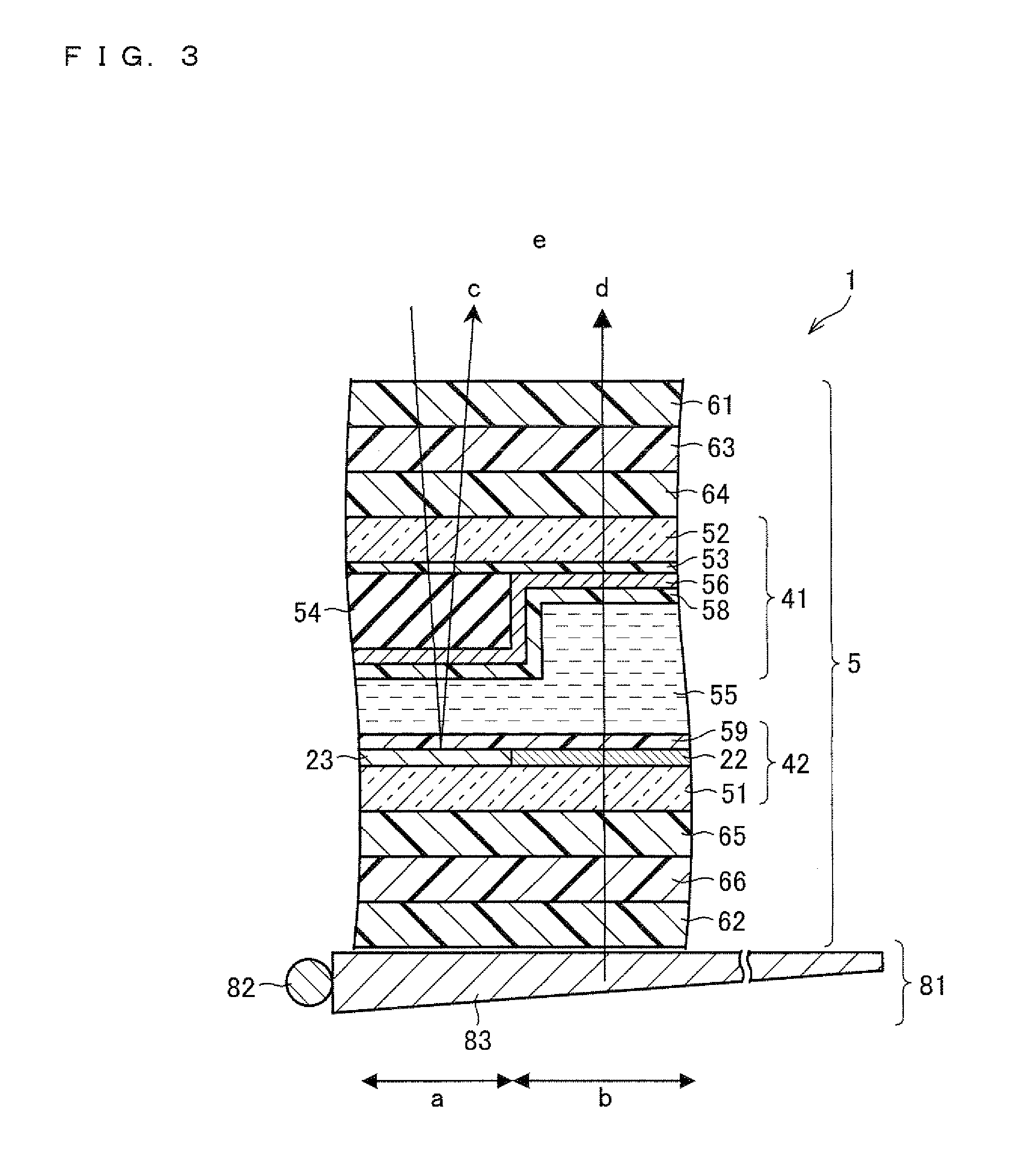
[0160]Embodiment 2 of the present invention is described below with reference to FIGS. 6 through 12. The present embodiment mainly deals with how Embodiment 2 differs from the Embodiment 1. For convenience of explanation, constituents which have similar functions to those explained in the Embodiment 1 are given identical reference numerals, and are not explained repeatedly.
[0161]The present embodiment is characterized in that the border line between a second transparent electrode 22 and a reflective electrode 23 is not a straight line. More specifically, the border line between the second transparent electrode 22 and the reflective electrode 23 has a bent section (step section, concavity and convexity), and one of the second transparent electrode 22 and the reflective electrode 23 has an area partially surrounded by the other one of the electrodes.
[0162](a) of FIG. 6, (a) of FIG. 7 and (a) of FIG. 8 are plan views each schematically illustrating an arrangement of a pixel 11 in a TFT...
embodiment 3
[0187]Embodiment 3 of the present invention is described below with reference to FIGS. 13 and 14. The present embodiment mainly deals with how the Embodiment 3 is different from the Embodiments 1 and 2. For convenience of explanation, constituents which have similar functions to those explained in the Embodiments 1 and 2 are given identical reference numerals, and are not explained repeatedly.
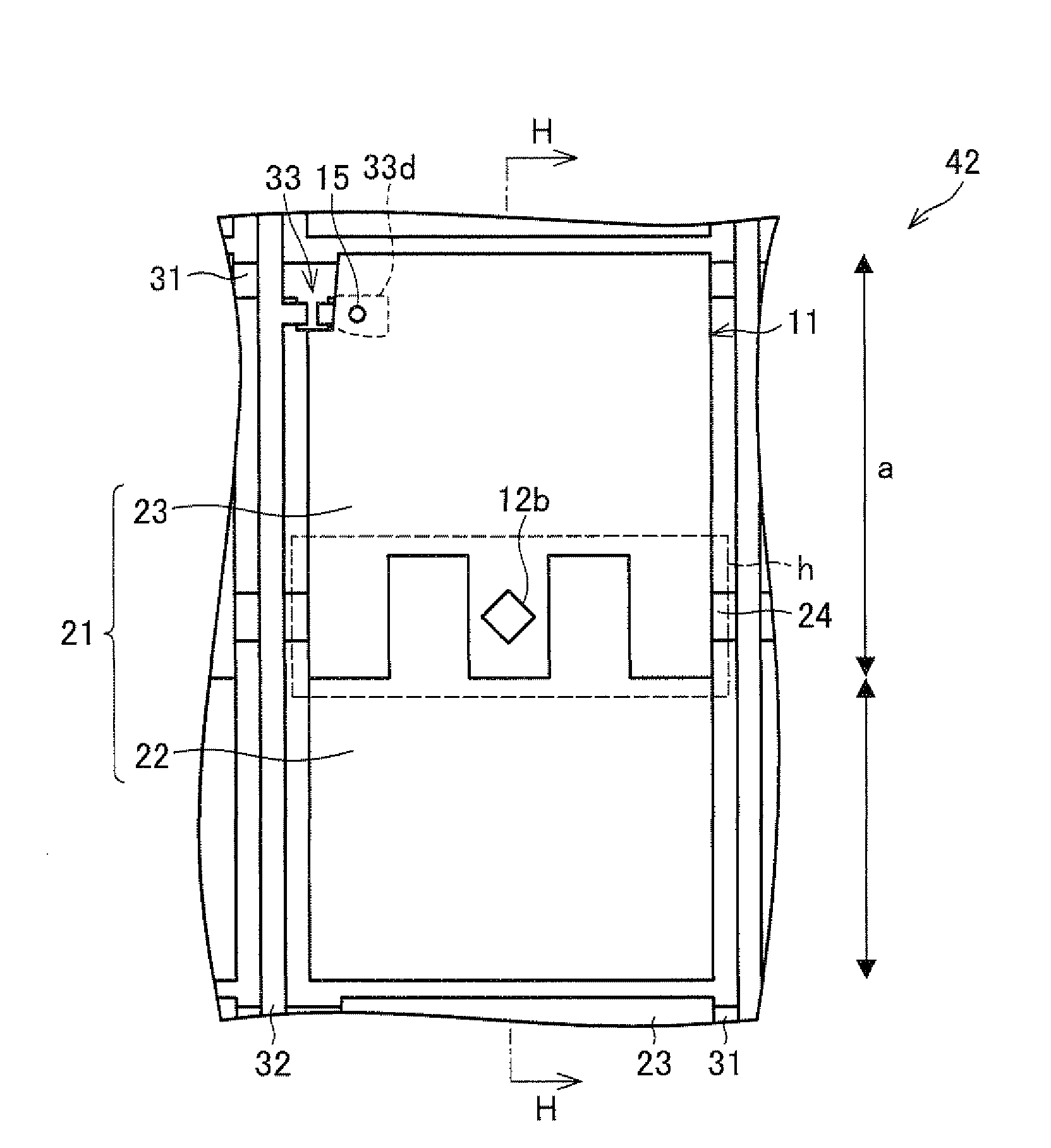
[0188]A feature of the present embodiment resides in that a slit 12a serving as the nucleus generation section is formed in a second transparent electrode 22, unlike the Embodiment 2. Other constituents are similar to those in the Embodiment 2.
[0189](a) of FIG. 13 is a plan view schematically illustrating an arrangement of a pixel 11 of a TFT substrate 42 in a liquid crystal display device 1 of the present embodiment in which a nucleus generation section is provided on a second transparent electrode 22. Further, (b) of FIG. 13 is a view showing an end surface of a reflective electrode 23 corres...
embodiment 4
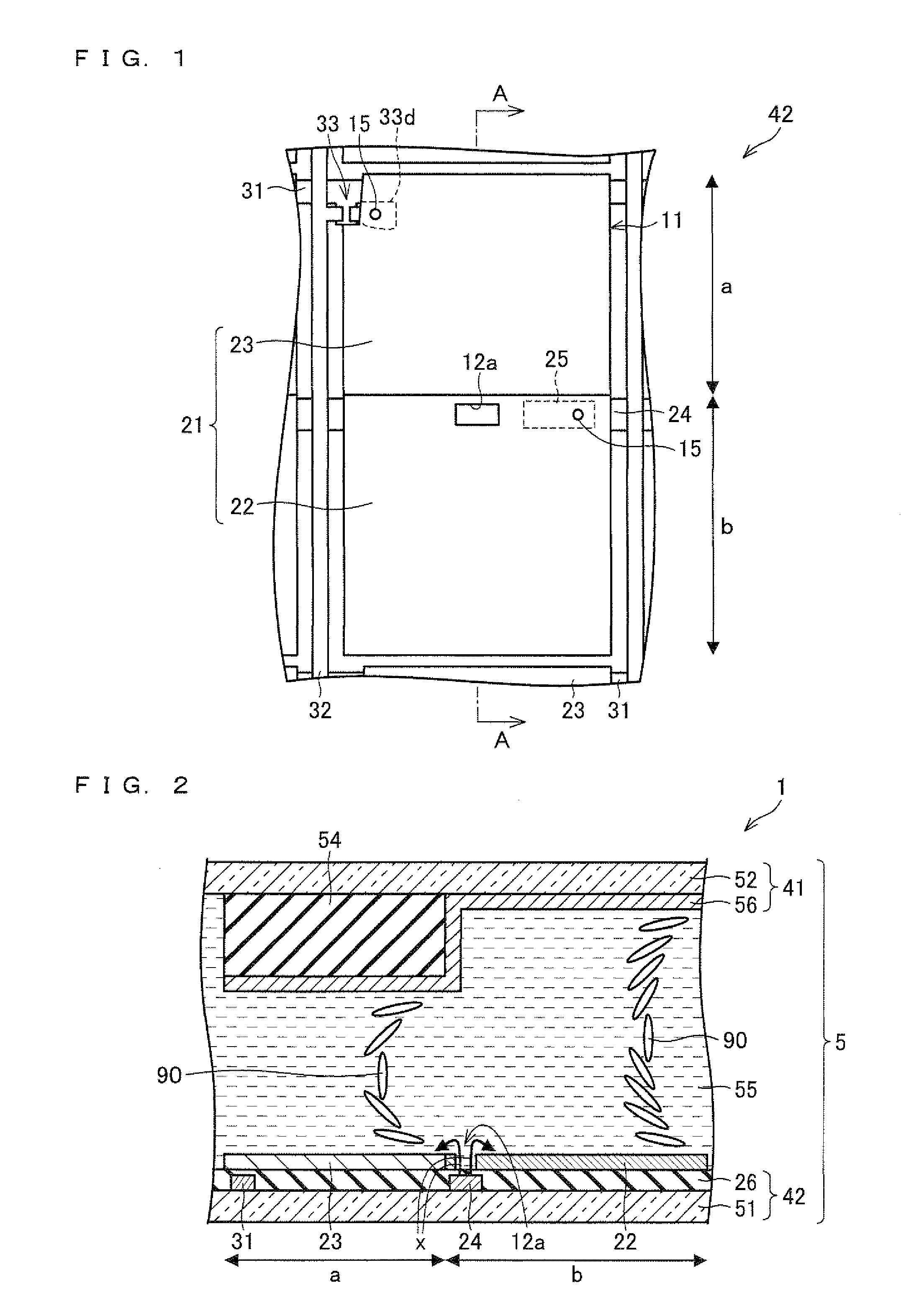
[0199]Embodiment 4 of the present invention is described below with reference to FIGS. 17 and 18. The present embodiment mainly deals with how the Embodiment 4 differs from the above embodiments. For convenience of explanation, constituents which have similar functions to those explained in the above embodiments are given identical reference numerals, and are not explained repeatedly.
[0200]A feature of the present embodiment resides in that the border line between a second transparent electrode 22 and a reflective electrode 23 has a rectangular shape, and in that the nucleus generation section is formed in a convex section of the second transparent electrode 22. In other words, the nucleus generation section is formed in an area of the second transparent electrode 22 which is sandwiched between two neighboring convex sections of the reflective electrode 23.
[0201]FIG. 17 is a plan view schematically illustrating an arrangement of a pixel 11 of a liquid crystal display device 1 of the...
PUM
| Property | Measurement | Unit |
|---|---|---|
| distance | aaaaa | aaaaa |
| distance | aaaaa | aaaaa |
| distance | aaaaa | aaaaa |
Abstract
Description
Claims
Application Information
 - R&D
- Intellectual Property
- Life Sciences
- Materials
- Tech Scout
- Unparalleled Data Quality
- Higher Quality Content
- 60% Fewer Hallucinations
Browse by: Latest US Patents, China's latest patents, Technical Efficacy Thesaurus, Application Domain, Technology Topic, Popular Technical Reports.
© 2025 PatSnap. All rights reserved.Legal|Privacy policy|Modern Slavery Act Transparency Statement|Sitemap|About US| Contact US: help@patsnap.com