Composite substrate and elastic wave device using the same

a technology of elastic wave and substrate, which is applied in the direction of generator/motor, sonic/ultrasonic/infrasonic transmission, transmission, etc., can solve the problems of device not being able to stand the temperature (about 260° c.) of the reflow process, poor production yield, etc., and achieves high heat resistance, high frequency temperature properties, and effective suppression of frequency temperature properties of piezoelectric substrates

Active Publication Date: 2010-07-22
NGK INSULATORS LTD
View PDF5 Cites 34 Cited by
  • Summary
  • Abstract
  • Description
  • Claims
  • Application Information

AI Technical Summary

Benefits of technology

[0010]According to the composite substrate of the invention, since the piezoelectric substrate is bonded, via the organic adhesive layer, to the silicon support substrate having a coefficient of thermal expansion smaller than that of the piezoelectric substrate, variation in the frequency temperature properties of the piezoelectric substrate can be effectively suppressed. Moreover, the heat resistance is higher than that of devices in which the support substrate is bonded to the piezoelectric substrate in the (100) plane or the (110) plane. For example, even when a reflow process is employed for mounting a surface acoustic wave device produced using the composite substrate on a mounting substrate, the occurrence of fracture in the surface acoustic wave device due to the tem...

Problems solved by technology

However, the prior art surface acoustic wave devices have posed a problem that fracture of devices sometimes occurs after the completion of a reflow process, resulting in a poor production yield.
The reasons for causing such a problem is th...

Method used


Image

  • Composite substrate and elastic wave device using the same
  • Composite substrate and elastic wave device using the same
  • Composite substrate and elastic wave device using the same

Examples


example 1

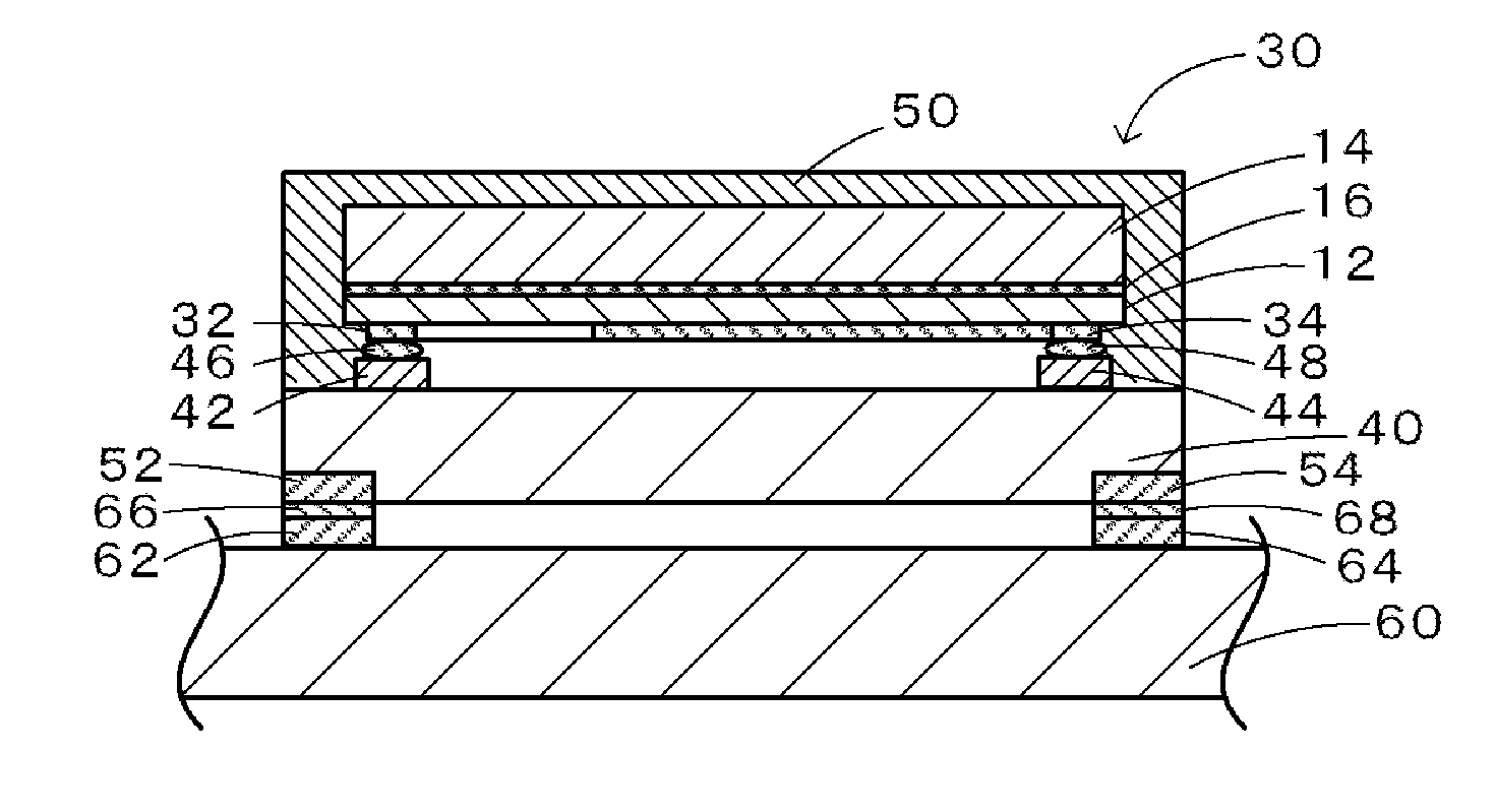
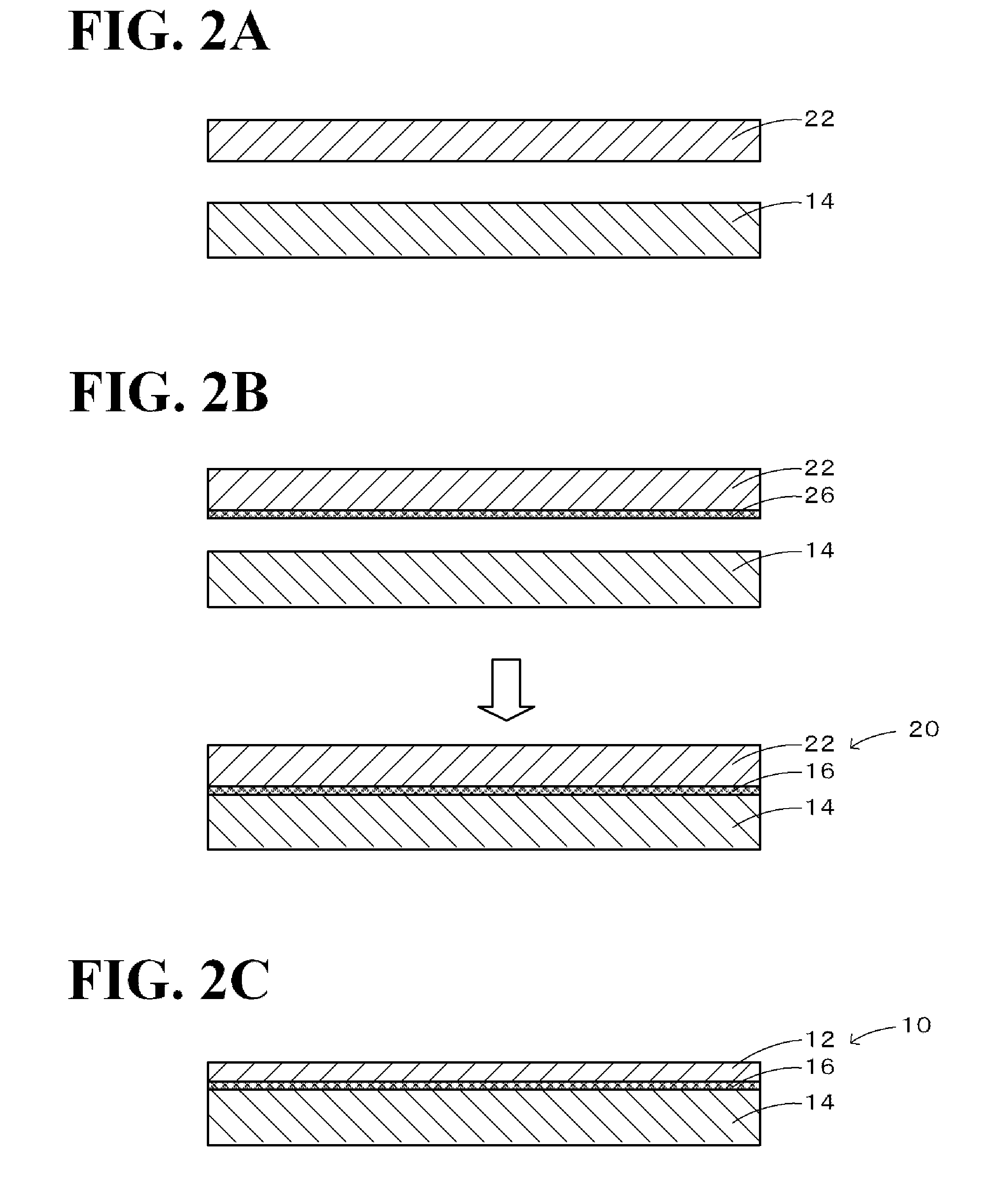
[0029]FIG. 1 is a perspective view of a composite substrate 10 of one example of the present invention. The composite substrate 10 is utilized for surface acoustic wave devices, and is formed in a round shape having one potion formed in a flat shape. The flat portion is referred to as an orientation flat (OF), and is used for, for example, detecting the position or direction of a wafer when various operations are performed in a process for producing surface acoustic wave devices. The composite substrate 10 has a piezoelectric substrate 12 containing lithium tantalate (LT) capable of transmitting a surface acoustic wave, a silicon support substrate 14 bonded to the piezoelectric substrate 12 in the (111) plane, and an adhesive layer 16 for bonding both the substrates 12 and 14. The piezoelectric substrate 12 has a diameter of 100 mm, a thickness of 30 μm, and a coefficient of thermal expansion of 16.1 ppm / K. The piezoelectric substrate 12 is a 42° Y cut X transmission LT substrate th...

example 2

[0040]A hundred composite substrates 10 were produced in the same manner as in Example 1, except that the thickness of the support substrate 14 was 250 μm and the adhesive layer 16 was obtained by solidification of acrylic resin in place of epoxy resin and had thickness of 0.6 μm.

example 3

[0045]A hundred composite substrates 10 were produced in the same manner as in Example 1, except that the thickness of the support substrate 14 is 200 μm, the thickness of the piezoelectric substrate 12 is 20 μm, and the adhesive layer 16 was obtained by solidification of acrylic resin in place of epoxy resin and had thickness of 0.6 μm.


PUM


Abstract

A composite substrate 10 includes: a piezoelectric substrate 12 capable of transmitting an elastic wave and composed of lithium tantalate (LT); a silicon support substrate 14 that is bonded to the rear surface of the piezoelectric substrate in the (111) plane; and an adhesive layer 16 bonding the substrates 12 and 14 to each other.

Description

BACKGROUND ART [0001]1. Field of the Invention[0002]The present invention relates to a composite substrate, and an elastic wave device using the same.[0003]2. Description of the Related Art[0004]As elastic wave devices, surface acoustic wave devices that can function as filters or resonators for use in, for example, cellular phones, Lamb wave devices or thin film resonators (FEAR: Film Bulk Acoustic Resonator) using a piezoelectric thin film, and the like are known. Surface acoustic wave devices have a structure in which a support substrate and a piezoelectric substrate that transmits a surface acoustic wave wave are bonded to each other and a comb shaped electrode capable of exciting a surface acoustic wave is provided on the front surface of the piezoelectric substrate. Thus, by bonding a support substrate having a coefficient of thermal expansion smaller than that of a piezoelectric substrate to the piezoelectric substrate, changes in the dimension of the piezoelectric substrate ...

Claims


Application Information

Patent Timeline
IPC IPC(8): H03H9/17H03H9/145
CPCH03H9/02015H03H9/02559H01L2224/0554H01L2224/16225H01L2924/00014H01L2224/05568H01L2224/05573H03H9/02574H03H9/059H03H9/1085H03H9/173H03H9/174H01L2224/05599H01L2224/0555H01L2224/0556
Inventor SUZUKI, KENJI
Owner NGK INSULATORS LTD
Why Eureka
Try Eureka