Inductance component

a technology of inductance components and components, applied in the direction of inductances, transformers/inductance coils/windings/connections, inductances/transformers/magnets, etc., can solve the problems of low reliability and low reliability of inductances, and achieve high reliability, increase saturation magnetic flux, and improve magnetic permeability

Active Publication Date: 2010-07-22
PANASONIC CORP
View PDF16 Cites 27 Cited by
  • Summary
  • Abstract
  • Description
  • Claims
  • Application Information

AI Technical Summary

Benefits of technology

[0011]According to another aspect of the present invention, the inductance component is preferably provided with a plurality of magnetic layers, and a portion of the element is interposed between the plurality of magnetic layers. According to the aspect of the invention, it becomes possible to increase a saturation magnetic flux, and at the same time, even when the thermal expansion rate between the element and the magnetic layers, as well as between the magnetic layers, is different, the magnetic layers are not detached from the element, and high reliability is realized.
[0012]According to still another aspect of the present invention, the inductance component is preferably formed such that at least a portion of the terminal is formed of the magnetic body. With this configuration, it becomes possible to improve magnetic permeability without increasing an area of the inductance component itself, or to decrease an occupation area of the coil, and as a result, an inductance value may be improved.
[0013]According to yet another aspect of the present invention, the inductance component is preferably formed such that a slit is formed on the magnetic layer and the slit is filled with a portion of the element. With this configuration, a stress is not locally applied to the magnetic body even in the condition where heat is applied to the entire component, such as when implementing soldering, and high reliability can be realized.
[0014]According to yet another aspect of the present invention, the inductance component is preferably formed such that a plurality of substantially V-shaped slits, spreading from a bending portion thereof in an outer

Problems solved by technology

However, such a conventional inductance component has a problem that reliability thereof is low.
That is to say, in the above-described conventional configuration, a stress is locally applied to the magn

Method used


Image

  • Inductance component
  • Inductance component
  • Inductance component

Examples


first embodiment

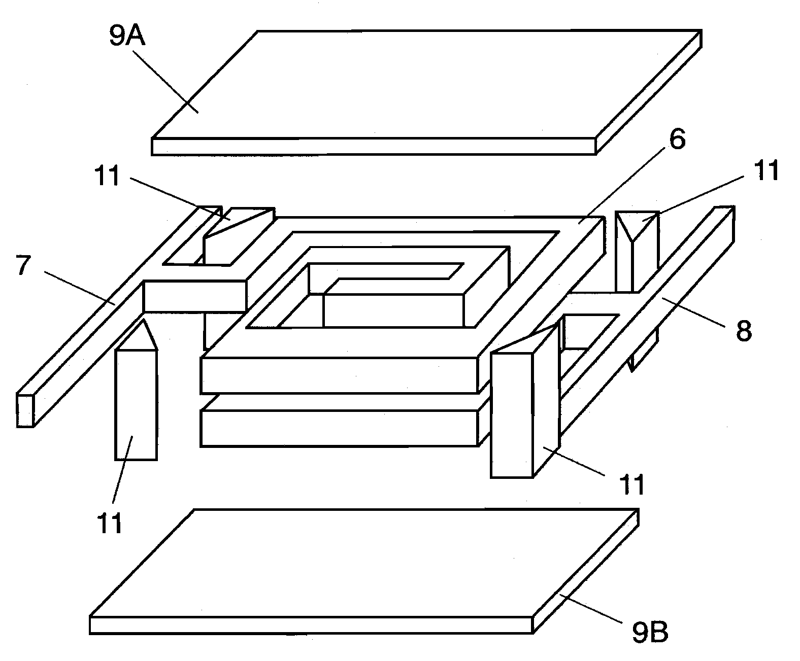
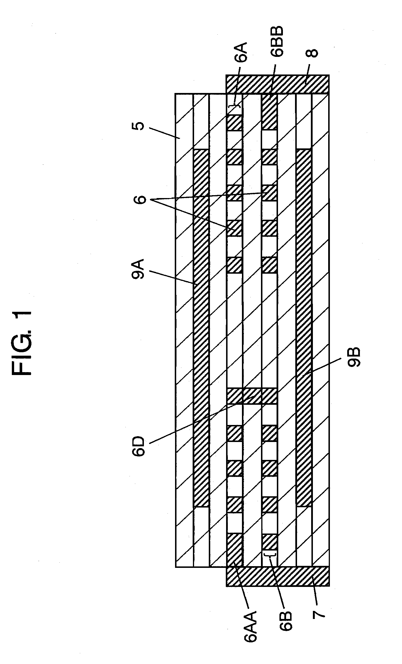
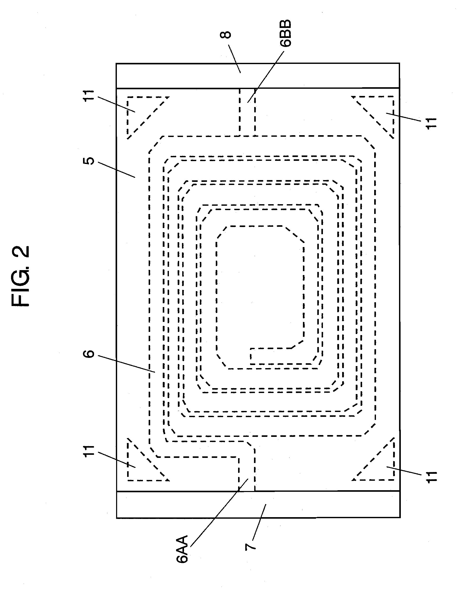
[0057]Hereinafter, an inductance component according to a first embodiment of the present invention is described with reference to FIG. 1 showing a cross-sectional view of the inductance component according to the first embodiment of the present invention, FIG. 2 showing a top view of the inductance component and FIG. 3 showing an exploded perspective view of the inductance component.

[0058]In FIG. 1, coil 6 is formed in sheet-shaped element 5, and terminals 7 and 8 are formed on an outer side of this coil 6, as shown in FIG. 2. As shown in FIG. 1, via 6D is formed between planar coils 6A and 6B, which form coil 6, in element 5, and magnetic layers 9A and 9B are formed on upper and lower sides of coil 6, respectively, in element 5.

[0059]Here, magnetic layers 9A and 9B are arranged so as to be substantially parallel to a winding surface of coil 6. This is in order to arrange magnetic layers 9A and 9B having high magnetic permeability in the path of a magnetic flux generated from coil ...

second embodiment

[0084]Next, an inductance component according to a second embodiment of the present invention is described with reference to the drawings. FIG. 5 is a cross-sectional view of the inductance component according to the second embodiment of the present invention.

[0085]In FIG. 5, coil 6 is formed in sheet-shaped element 5, terminals 7 and 8 are formed on an outer portion of this coil 6, and via 6D is formed between planar coils 6A and GB, which form coil 6, in element 5. Portions of terminals 7 and 8 are formed of magnetic terminals 7A and 8A formed of a magnetic body.

[0086]Here, it is preferred that a metal magnetic material containing Fe or an Fe-alloy is used as a material of magnetic terminals 7A and 8A from the viewpoint of the magnetic flux density and the magnetic loss. In a case where the Fe-alloy is used as magnetic terminals 7A and 8A, it is preferred to make the composition ratio of Fe not less than 30 percent by mass. This is because the magnetic characteristic of high satur...

third embodiment

[0099]Hereinafter, an inductance component according to a third embodiment of the present invention is described with reference to the drawings. FIG. 7 is a cross-sectional view of the inductance component according to the third embodiment of the present invention.

[0100]In FIG. 7, coil 27 is formed in sheet-shaped element 26, terminals 28 and 29 are formed on outermost peripheral portions of this coil 27, and via 27C is formed between planar coils 27A and 27B, which form coil 27, in element 26.

[0101]Magnetic layers 30A and 30B, and 30C and 30D are formed on upper and lower sides of coil 27 in element 26, respectively.

[0102]Portions of terminals 28 and 29 are formed of magnetic terminals 28A and 29A formed of a magnetic body.

[0103]Further, in the present embodiment, magnetic terminals 28A and 29A in terminals 28 and 29 are formed also on the upper and lower surfaces of element 26.

[0104]On an inner portion of coil 27 in element 26, magnetic center core 31 formed of a magnetic body is ...


PUM


Abstract

In an inductance component, a stress is not locally applied even in the condition where heat is applied to entire component, such as when implementing soldering, so that high reliability is realized. For realizing this, the component includes element (5), coil (6) formed in element (5), terminals (7, 8) electrically connected to coil (6), and magnetic layers (9A, 9B) arranged so as to be substantially parallel to a winding surface of coil (6) are formed in element (5) and entire magnetic layers (9A, 9B) is covered with a material of which thermal expansion and contraction rates are constant.

Description

TECHNICAL FIELD[0001]The present invention relates to an inductance component used in a power supply circuit of a cellular phone, for example.BACKGROUND ART[0002]Conventionally, the inductance component of this kind is configured as a chip coil in which coil 2 is formed in sheet-shaped element 1, terminal 3 is electrically connected to coil 2, and magnetic layers 4 are formed on upper and lower surfaces of element 1, as shown in FIG. 23.[0003]By providing insulating covering 20 so as to cover magnetic layer 4 and entire element 1, electric connection with other components is prevented.[0004]As the conventional art document information regarding the present application, Patent Document 1 is known, for example.[0005]However, such a conventional inductance component has a problem that reliability thereof is low.[0006]That is to say, in the above-described conventional configuration, a stress is locally applied to the magnetic layer 4 by heat when implementing soldering or the like, fro...

Claims


Application Information

Patent Timeline
IPC IPC(8): H01F27/29
CPCH01F17/0006H01F17/0013H01F27/002H01F27/365H01F41/046H01F2017/0066H01F2017/008H01F2017/048H01F27/36H01F27/366
Inventor ISHIMOTO, HITOSHIMATSUTANI, NOBUYAUEMATSU, HIDENORISHIMOYAMA, KOJIOHBA, MICHIOTAOKA, MIKIO
Owner PANASONIC CORP
Why Eureka
Try Eureka