Method of transferring a device and method of manufacturing a display apparatus

a technology of transfer device and manufacturing method, which is applied in the direction of electrical apparatus, chemistry apparatus and processes, semiconductor devices, etc., can solve the problems of difficult to design a material with a sufficient bonding force, narrow laser energy transfer range, and low degree of flexibility in selecting light absorbing layer and release layer selection, etc., to achieve convenient ablation, ensure bonding property, and transfer device reliable

Inactive Publication Date: 2010-07-29
SONY CORP
View PDF3 Cites 144 Cited by
  • Summary
  • Abstract
  • Description
  • Claims
  • Application Information

AI Technical Summary

Benefits of technology

[0010]Since in such a structure, the release layer provided on the device side with respect to the bonding layer is ablated and the device (light emitting diode) is transferred from the first substrate onto the second substrate, the device is transferred to the second substrate side without the bonding layer left on the device side. In addition, by providing the bonding layer and the release layer separately, it is possible to reliably transfer the device owing to the release layer that has a wide appropriate range of laser energy for ablation and is easy to be ablated while sufficiently ensuring bonding property between the first substrate and the device owi

Problems solved by technology

Therefore, there arise problems that a degree of flexibility in selection of the light absorbing layer and the release layer is low and an appropriate range of laser energy capable of being transferred is narrow.
Consequently, it h

Method used


Image

  • Method of transferring a device and method of manufacturing a display apparatus
  • Method of transferring a device and method of manufacturing a display apparatus
  • Method of transferring a device and method of manufacturing a display apparatus

Examples


first embodiment

1. First Embodiment

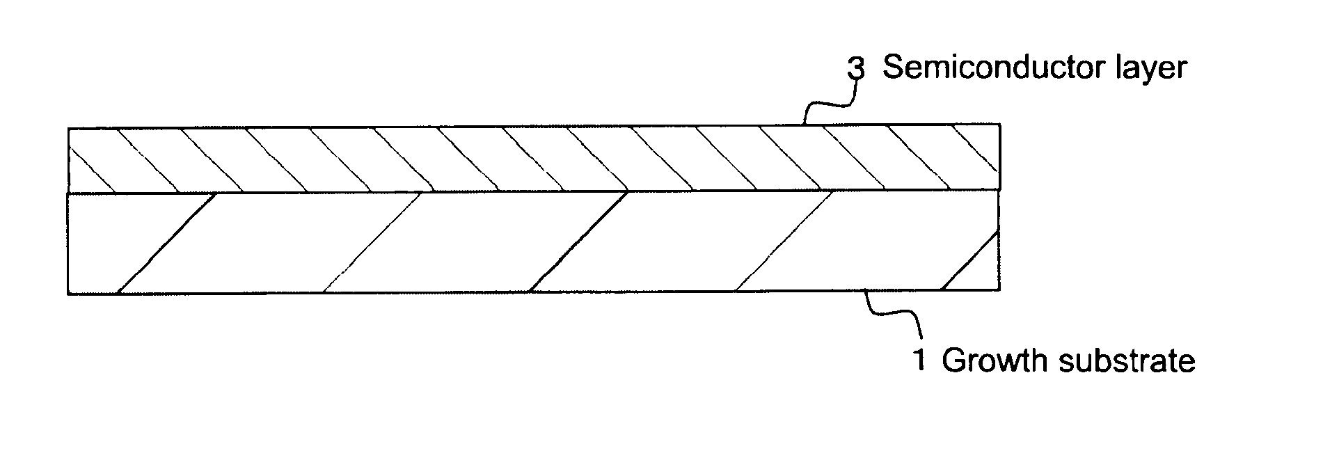
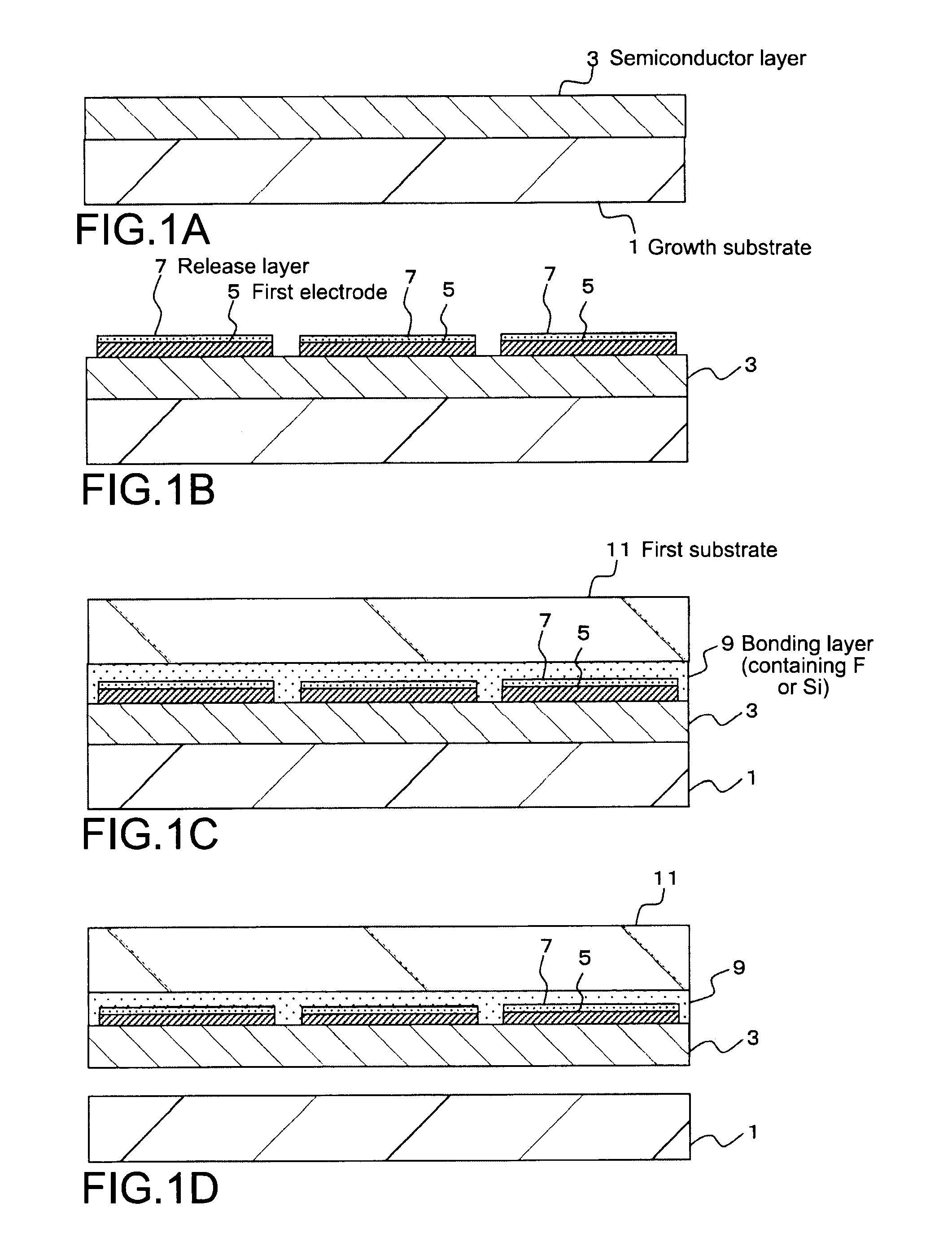
[0023]First, as shown in FIG. 1A, a semiconductor layer 3 having a layer structure is epitaxially grown on a substrate 1 for growing semiconductor crystal (hereinafter, referred to as growth substrate 1), the growth substrate 1 being made of sapphire or the like. Here, a compound semiconductor layer of a first conductivity type (for example, n-type), an active layer, and a compound semiconductor layer of a second conductivity type (for example, p-type) are first epitaxially grown by a crystal growth method such as an MO-CVD method in the stated order, to thereby form the semiconductor layer 3.

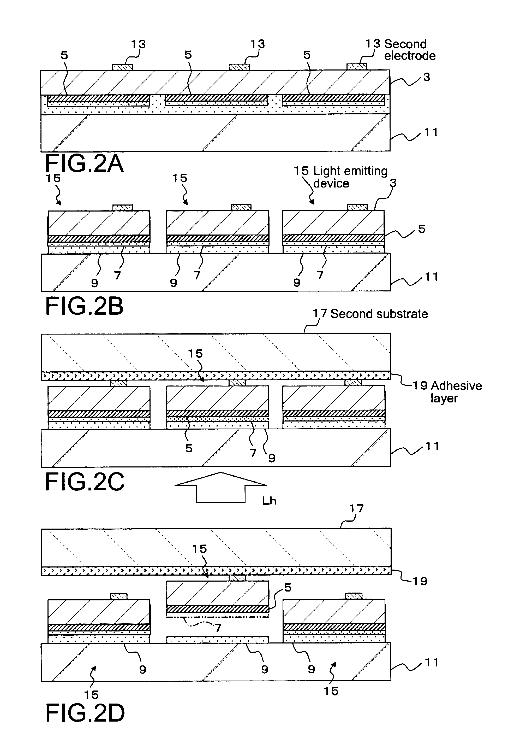
[0024]Next, as shown in FIG. 1B, first electrodes 5 and release layers 7 are formed and arranged on the semiconductor layer 3.

[0025]Each of the first electrodes 5 is a second conductivity type electrode (for example, p-electrode) and is formed to have a layer structure in which platinum (Pt) and gold (Au) are laminated on nickel (Ni). Further, in a case where the first electr...

second embodiment

2. Second Embodiment

[0055]A second embodiment shown in FIGS. 5 and 6 is different from the first embodiment in the manufacturing procedure up to the process of laminating and arranging in the stated order the release layers 7 and the light emitting devices 15 on the first substrate 11 having light transmitting property, via the bonding layer 9 having light transmitting property. The processes subsequent to that process are the same as those in the first embodiment. Hereinafter, the manufacturing procedure of the second embodiment will be described with reference to FIGS. 5 and 6. It should be noted that descriptions overlapping with the first embodiment will be omitted.

[0056]First, as shown in FIG. 5A, the compound semiconductor layer of the first conductivity type (for example, n-type), the active layer, and the compound semiconductor layer of the second conductivity type (for example, p-type) are epitaxially grown in the stated order on the growth substrate 1 for growing semicondu...


PUM


Abstract

A method of transferring a device includes: arranging a release layer and a device in the stated lamination order on a first substrate having light transmitting property via a bonding layer having light transmitting property; arranging an adhesive layer formed on a second substrate so that the adhesive layer is opposed to a surface of the first substrate on which the device is arranged; and ablating the release layer by performing light irradiation on the release layer from the first substrate side and transferring the device onto the second substrate with the bonding layer being left on the first substrate.

Description

BACKGROUND OF THE INVENTION[0001]1. Field of the Invention[0002]The present invention relates to a method of transferring a device and a method of manufacturing a display apparatus, and more particularly, to a method of transferring a device from a first substrate side to a second substrate side by an ablation technique and a method of manufacturing a display apparatus using the method of transferring a device.[0003]2. Description of the Related Art[0004]In the manufacture of a display apparatus in which light emitting diodes (LEDs) are arranged, a process of transferring the LEDs, which are arranged on a wafer at a fine pitch, onto an apparatus substrate in a state where the LEDs are rearranged in accordance with an enlarged pitch corresponding to a pixel array is conducted. This transfer process, to which an ablation technique is applied, is conducted as follows, for example.[0005]First, devices (light emitting diodes) are arranged on a release layer formed on a first substrate, t...

Claims


Application Information

Patent Timeline
IPC IPC(8): B32B37/02
CPCH01L25/0753H01L27/1214H01L27/1266H01L33/0079H01L24/19H01L2924/12041H01L2924/15788Y10T156/1041H01L2924/00H01L33/0093H01L2224/73267H01L2224/92244H01L2224/04105
Inventor TOMODA, KATSUHIRO
Owner SONY CORP
Why Eureka
Try Eureka