

Lithographic imaging with printing members having metal imaging bilayers
a technology of metal imaging and printing members, which is applied in the field of lithographic imaging with printing members having metal imaging bilayers, can solve the problems of difficult to retain adequate adhesion to adjacent layers, catastrophic overheating, etc., and achieves low emissivity of imaging radiation, high transmittance, and high extinction coefficient.
- Summary
- Abstract
- Description
- Claims
- Application Information
AI Technical Summary
Benefits of technology
Problems solved by technology
Method used
Image

Examples
example 1
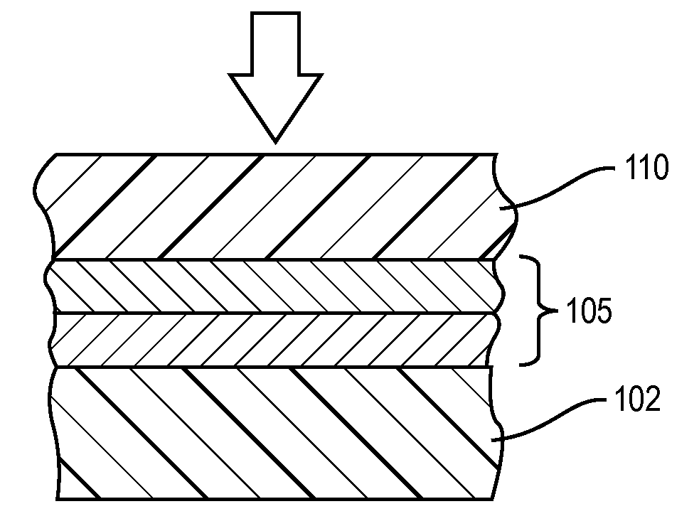
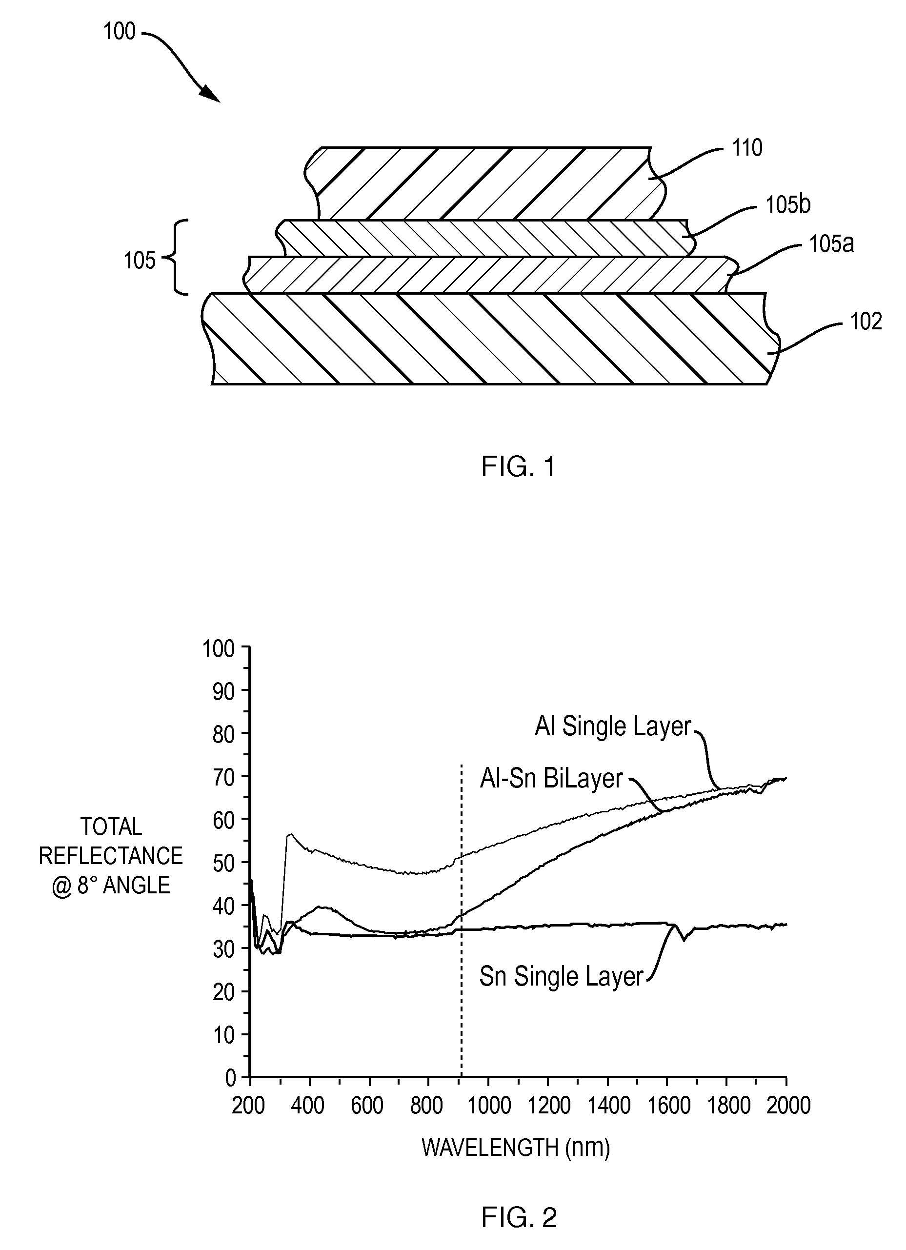
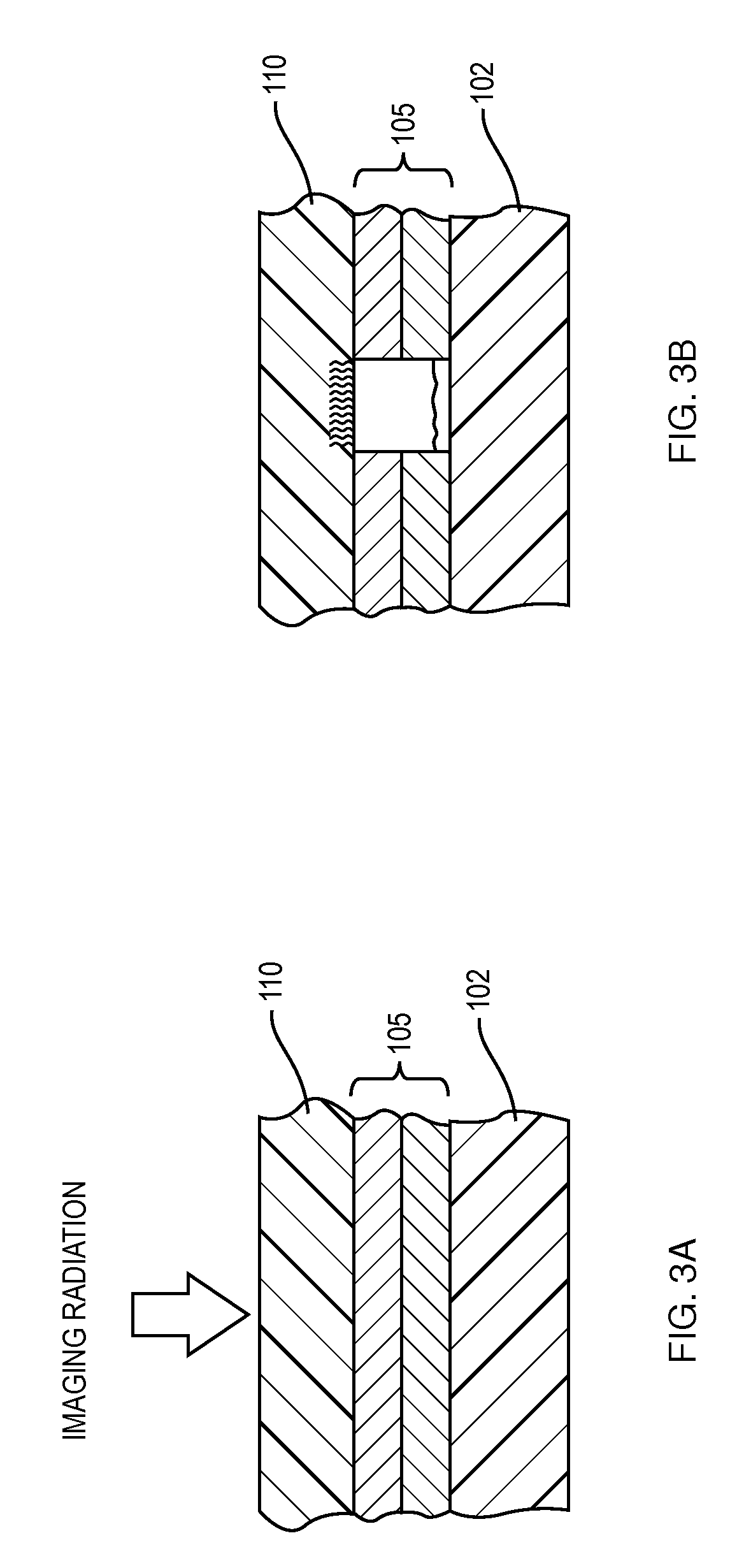
[0057]A dry printing member in accordance with the invention includes a polyester substrate having dispersed therein a highly scattering filler material (e.g., BaSO4, TiO2, etc.) at a loading level of 10% or less by weight. In this example, the substrate is a 200 μm polyethylene terephthalate film, sold by duPont—Teijin Films (Hopewell, Va.) under the trade name MELINEX 927W, which contains a dispersion of BaSO4 particles and provides a highly scattering base; the first radiation-responsive layer 105a is Al; and the second (upper) layer radiation-responsive layer 105b is Sn.
[0058]Deposition of the Al and Sn layers is carried out in a DC magnetron sputtering source using ultrahigh purity argon as the sputtering gas. Prior to the metal deposition, the sputtering chamber is evacuated to base pressures below 3×10⁻⁵ Torr and back-filled with argon up to a pressure of 5 mTorr. The Al and Sn layers are sequentially sputterred to yield layers of thicknesses 10 nm and 4 nm, respectively.
[005...
example 2
[0062]This example describes a negative-working dry printing plate that includes a silicone layer disposed above the structure described in Example 1. The silicone layer has a highly crosslinked network structure produced by addition or hydrosilylation reaction between vinyl-functional silicones and a silicon hydride crosslinker. The silicone solutions used in this example are described below, but other suitable formulations are also given in previous patents, e.g., U.S. Pat. No. 5,212,048, the entire disclosure of which is hereby incorporated by reference.
ComponentSupplierParts165K & 10KNusil Silicone Technology, Charlotte, NC0.12SiliconeDC Syl-offUnivar USA Inc., Atlante, GA8.557367CPC072Umicore Precious Metals, S. Plainfield, NJ0.38HeptaneHoughton Chemicals, Allston, MA90.95
[0063]The coating solution is applied on the imaging member using a wire-wound rod, then dried and cured to produce a uniform silicone coating of 1.1 g / m2. The printing plate is then ready for imaging. The pla...
example 3
[0067]This example is similar to Example 2 with radiation-responsive and oleophobic layers disposed on highly scattering polyester base and laminated to an aluminum coil. The structure described in Example 1 was constructed using the 50 μm Melinex 928W polyester substrate, and then coated with the 1.1 g / m2 formulation used in Example 2. The coated structure was then laminated to a 150 μm coil of aluminum 3103 alloy lithographic metal (Alcoa, Pittsburgh, Pa.) using an acrylate adhesive supplied by Dyna-Tech Adhesives & Coatings, Grafton, W.Va. The acrylate adhesive is a 100% solids formulation cured with an e-beam radiation source.
[0068]The printing plate was evaluated for imaging and printing performance using the equipment and procedures described in Example 2. The plate exhibits imaging and press performance similar to that of the plate member of Example 2.
PUM
| Property | Measurement | Unit |
|---|---|---|
| wavelength range | aaaaa | aaaaa |
| transmittance | aaaaa | aaaaa |
| melting points | aaaaa | aaaaa |
Abstract
Description
Claims
Application Information