Method of performing hyperspectral imaging with photonic integrated circuits

a photonic integrated circuit and hyperspectral imaging technology, applied in the field of hyperspectral imagers, can solve problems such as the total intensity of electromagnetic radiation incident beams

Active Publication Date: 2010-07-29
UNIV OF WASHINGTON
View PDF3 Cites 36 Cited by
  • Summary
  • Abstract
  • Description
  • Claims
  • Application Information

AI Technical Summary

Problems solved by technology

One limitation of such devices, however, is that they only detect the total intensity of an incident beam of electromagnetic radiation.

Method used


Image

  • Method of performing hyperspectral imaging with photonic integrated circuits
  • Method of performing hyperspectral imaging with photonic integrated circuits
  • Method of performing hyperspectral imaging with photonic integrated circuits

Examples


Embodiment Construction

[0070]We now describe high index contrast waveguides that are useful to concentrate light in order to enhance nonlinear optical effects in various materials so that such effects can be employed to manipulate light (or more generally electromagnetic radiation) at low power levels, as compared to conventional systems and methods that employ nonlinear optical materials. The manipulation of electromagnetic radiation or light can be useful to provide a variety of components that perform operations on light such as rectification, modulation, filtering, and logic operations in a manner analogous to the same operations which are provided using electronic devices operating on electrical signals. For example, an input light wave to be processed is impressed onto the component. The light wave has at least one parameter characterizing the light wave, such as one of an intensity, a polarization, a frequency, a wavelength, and a duration (e.g., a pulse length, or in the case of continuous wave li...


PUM


Abstract

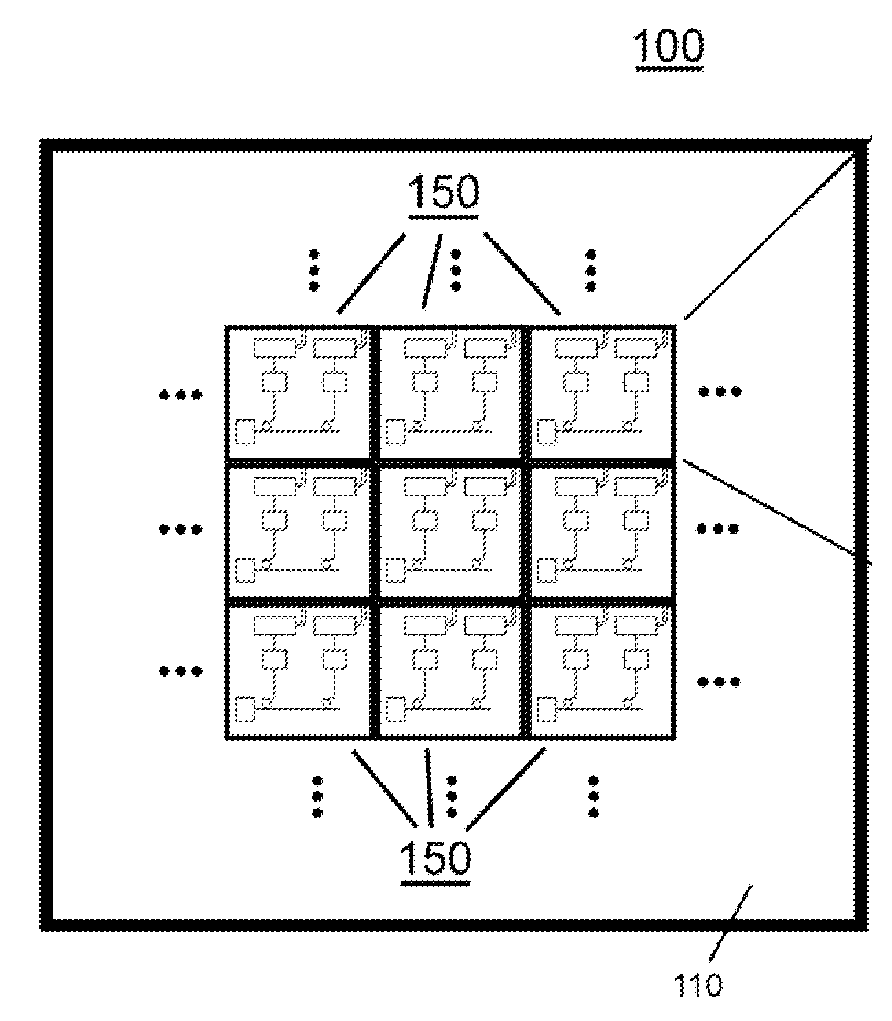
According to the invention, an integrated hyperspectral imager includes a planar photonic substrate. A plurality of imaging pixel photonic circuits is disposed in a M×N array on the planar photonic substrate. Each imaging pixel photonic circuit includes an input coupler configured to receive a broadband input electromagnetic radiation. A waveguide is optically coupled to the input coupler. A plurality of wavelength filters is optically coupled to the waveguide. Each wavelength filter has a wavelength filter input and a wavelength filter output. Each detector has a detector input optically coupled respectively to each of the wavelength filter outputs. Each detector has a respective detector output. The integrated hyperspectral imager is configured to provide electrical signals that are representative of a hyperspectral image of the received broadband input electromagnetic radiation. A method for recording an image based on a received electromagnetic radiation is also described.

Description

CROSS-REFERENCE TO RELATED APPLICATIONS[0001]This application claims priority to and the benefit of co-pending U.S. provisional patent application Ser. No. 61 / 084,513, filed Jul. 29, 2008, which application is incorporated herein by reference in its entirety.FIELD OF THE INVENTION[0002]The invention relates to a hyperspectral imager in general and more particularly to a hyperspectral imager photonic integrated circuit.BACKGROUND OF THE INVENTION[0003]CCD and CMOS imaging integrated circuits (IC) as well as other conventional imaging ICs are commonly used to capture images in real-time at visible and other wavelengths. Imaging ICs commonly form the basis for many modern photographic and video recording devices. One limitation of such devices, however, is that they only detect the total intensity of an incident beam of electromagnetic radiation.[0004]An existing enhancement to conventional IC imaging arrays of the prior art is the ability to detect not just an image, but to detect the...

Claims


Application Information

Patent Timeline
Patent Type & Authority Applications(United States)
IPC IPC(8): H01L27/146
CPCG02B6/12004G02B6/12007H01L27/14629H01L27/14627H01L27/14621
Inventor HOCHBERG, MICHAEL J.BAEHR-JONES, TOM
Owner UNIV OF WASHINGTON
Why Eureka
Try Eureka