Wavelength division image measuring device

a wavelength division and image technology, applied in the direction of optical radiation measurement, interferometric spectrometry, instruments, etc., can solve the problems of difficult to realize very sharp wavelength transmission characteristics, difficult to provide ink or resist type color filters with sharp wavelength selection characteristics, etc., to achieve easy integration, increase the number of wavelengths, and sharp selectivity

Inactive Publication Date: 2009-05-07
TOHOKU TECHNO ARCH CO LTD +1
View PDF1 Cites 25 Cited by
  • Summary
  • Abstract
  • Description
  • Claims
  • Application Information

AI Technical Summary

Benefits of technology

[0017]The wavelength selection filter according to the configuration of the present invention allows a measurement target light to be divided into a plurality of wavelength components with very sharp selectivity. Integration of the wavelength filter array composed of this configuration with the light receiving element array, such as CCD, makes it possible to obtain the spatial distribution for every narrow-band wavelength component contained in the measurement light by one-time imaging, which has been difficult to achieve by the conventional technology. An increase in kinds of filter elements to be arrayed allows an increase in the number of wavelengths to be divided as well. Additionally, since only the wavelength filter array and the light receiving element array are used, integration is easily achieved, resulting in small-sizing. Further, even when the wavelength band itself to be the measurement target is greatly changed, design and production of the filter array can be realized according to common guidelines and processes. The wavelength division image measuring device using such a wavelength filter array has wide industrial applications, and can offer image measurement functions, which are not provided by the conventional color image sensors.

Problems solved by technology

Meanwhile, although a so-called array of wavelength filters, in which a large number of microscopic filter elements with different wavelength characteristics are adjacently arranged, has a large number of application fields as described later, only an array with limited characteristics has been realized due to the difficulty in its production.
In general, an ink or resist type color filter is difficult to provide with sharp wavelength selection characteristics.
Thereby, it is difficult to realize very sharp wavelength transmission characteristics.
This method has problems that an optical system becomes complicated due to requiring a large number of optical elements, precise alignment between the optical elements is needed for matching the separated images of each wavelength with each other, or the like.
This method has problems that the photographing of high-speed phenomenon is difficult because of requiring considerable time until one synthesized image is obtained, it is inapplicable to measurement susceptible to vibration because of containing movable parts, the device is large-sized, or the like.
Meanwhile, it contains a serious problem that the degree of flexibility in designing wavelength characteristics is restricted due to the material constant of the light receiving element, for example, when the material system and principle of the light receiving element are changed, such as an infrared ray, the fundamental search of material process is needed to realize the filter characteristics, or the like.
This is caused by the fact that it is impossible to independently design the wavelength filter and the light receiving element.
Furthermore, it is not possible to obtain the spatial distribution for every narrow-band wavelength component contained in measurement light by one-time imaging.
However, since it is required that the CCD layer of the foundation not to be damaged by forming the multilayer film in this method, limitation on conditions of sputtering and etching for the self-cloning method is imposed thereon, resulting in a problem that a realizable periodic structure is restricted.
As described above, there is a problem that distinct spectrum separation is difficult in the method described in this document.

Method used


Image

  • Wavelength division image measuring device
  • Wavelength division image measuring device
  • Wavelength division image measuring device

Examples


first embodiment

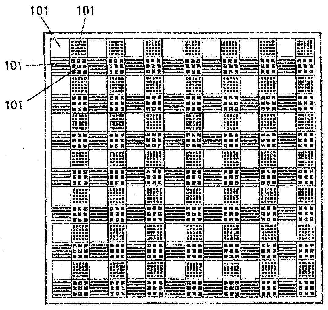
[0109]FIG. 4 is a diagram showing one embodiment of the present invention. An embodiment using edge filter characteristics of the photonic crystal in a visible wavelength band is illustrated here. A mask layer composed of 200 nm thick Cr is formed on a quartz substrate 401 by a sputtering method to then apply a photoresist thereon. Four lattice shapes are drawn thereon by a direct lithography using an electron beam. Namely, squares with the lattice spaces of 420 nm in a region 402, 440 nm in a region 403, 460 nm in a region 404, and 480 nm in a region 405 are formed in a square lattice arrangement manner. Areas of respective regions are set to squares of 5 micrometers on a side. Subsequently, the mask of chromium (Cr) is removed by RIE (reactive ion etching) after developing the photoresist to then transfer the pattern to the quartz substrate. An etching depth of the quartz substrate is set at 100 nm.

[0110]Subsequently, after forming a transition layer 406 composed of a quartz for c...

second embodiment

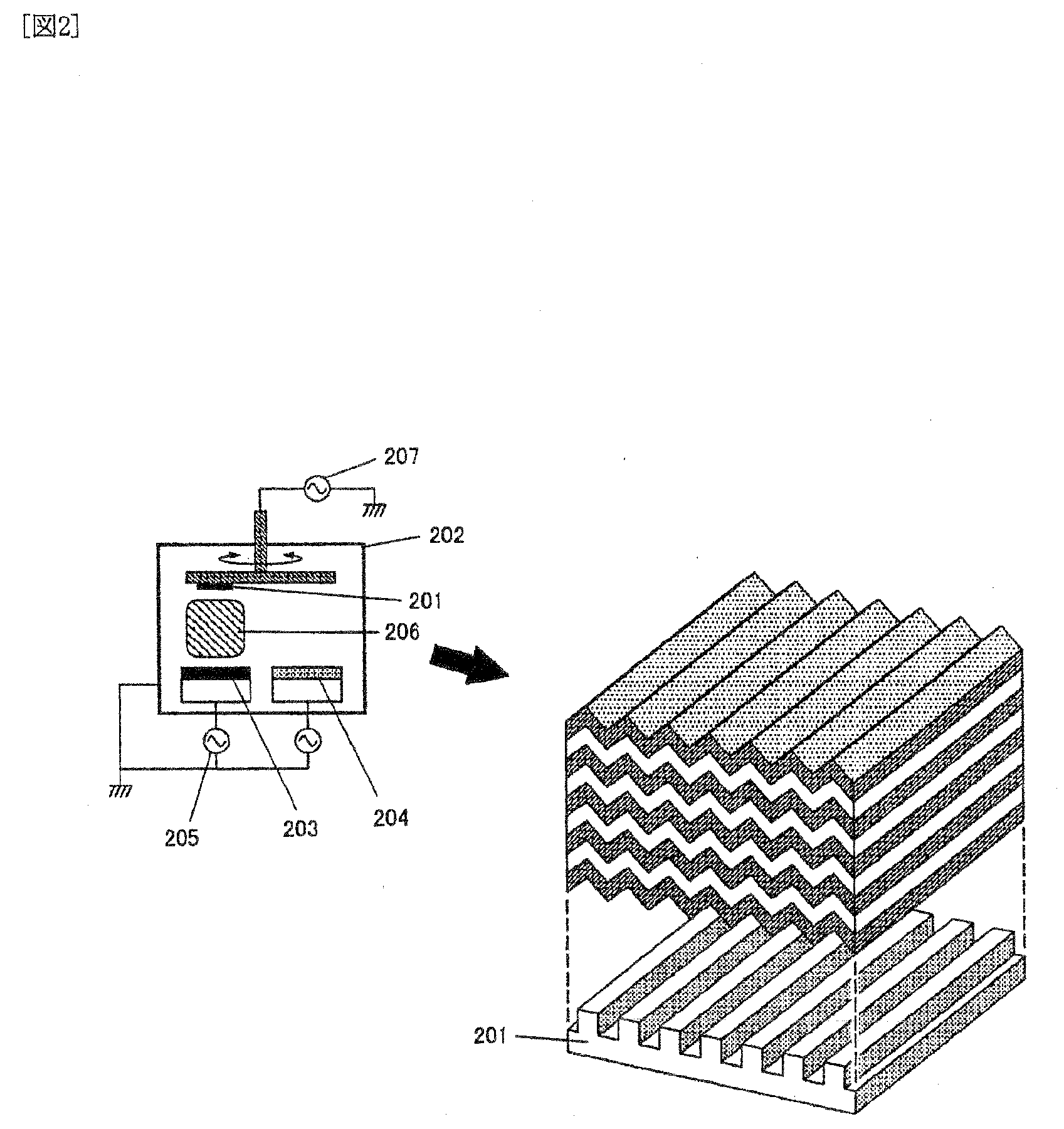
[0113]A second embodiment of the present invention is shown in FIG. 9. The present embodiment illustrates a method for using narrow-band wavelength selection characteristics of the photonic crystal. In this embodiment, the lattice shape of a substrate and its production method, and the method of forming a multilayer film by the self-cloning method are the same as those of the first embodiment, but the in-plane lattice period and the film constitution of the multilayer film are different therefrom. Namely, four regions 901, 902, 903, and 904 whose in-plane lattice constants are 200 nm, 250 nm, 300 nm, and 350 nm, respectively, are formed as the element regions of the filter. In the film thickness direction, a Ta2O5 layer 906 of 95.2 nm thickness and an SiO2 layer 907 of 133.3 nm thickness are alternately laid up to a total of 20 layers on a quartz substrate 905, and a Ta2O5 layer 908 of 133.3 nm thickness is subsequently laid as a cavity layer. Subsequently, a SiO2 layer of 133.3 nm ...

third embodiment

[0115]FIG. 11 is a diagram showing a third embodiment of the present invention. Namely, this embodiment is a combination of a filter 1101 in the aforementioned first or second embodiment (this is referred to as a “first filter” only in this embodiment) and a second wavelength filter 1102 which is not arrayed, namely, having uniform wavelength characteristics across a whole incident plane. An example of wavelength characteristics of a second filter is shown in FIG. 12. Since this has a uniform structure across the whole area, special ideas are not required for designing and manufacturing it. When the region 404 of the filter shown in the first embodiment is used as the first filter, combined transmission characteristics of both filters will be shown in FIG. 13. Namely, when the measurement light with the wide wavelength width ranging from 700 nm to 950 nm of wavelength is entered, wavelength components equal to or less than 770 nm of wavelength are also transmitted in the first embod...


PUM


Abstract

A wavelength division image measuring device that can divide a wideband incident light from a measurement object into a plurality of wavelengths with high selectivity to thereby measure these images simultaneously and collectively. Micro periodic irregular lattices are formed on a substrate 302. At this time, a plurality of microscopic element areas 101 with different lattice shapes and lattice periods are repeatedly arranged within a plane of the substrate 302. Next, a high refractive index material and a low refractive index material are alternately laid thereon so as to form a multilayer using a bias spatter method to thereby form a wavelength filter 301 with a photonic crystal structure. Thus, an array of the photonic crystal wavelength filters 031 with a sharp selectivity and different wavelength transmission characteristics can be obtained.

Description

TECHNICAL FIELD[0001]The present invention relates to a wavelength division image measuring device. More particularly, the present invention relates to an array of wavelength filters composed of microscopic element regions having different in-plane periodic shapes, and a measuring device of color distribution information using the same. Moreover, the present invention relates to a wavelength division image measuring device to allow a real-time wavelength division image measurement capable of obtaining a spatial distribution for every narrow-band wavelength component contained in measured light by one-time imaging.BACKGROUND ART[0002]Patent Document 1: Japanese Unexamined Patent Publication (Kokai) No. 2004-325902[0003]Patent Document 2: Japanese Unexamined Patent Publication (Kokai) No. 2004-341506[0004]Patent Document 3: Japanese Patent Publication No.[0005]Patent Document 4: Japanese Unexamined Patent Publication (Kokai) No. 2005-26567[0006]A wavelength filter is an element in whi...

Claims


Application Information

Patent Timeline
Patent Type & Authority Applications(United States)
IPC IPC(8): G01J3/45G02B5/22
CPCG01J3/02G01J3/0205G01J3/0259G01J3/36G02B27/142G01J3/513G01J2003/1213G02B27/1006G02B27/1073G01J3/51
Inventor OHTERA, YASUOTAKASHI, SATOSHOJIRO, KAWAKAMI
Owner TOHOKU TECHNO ARCH CO LTD
Why Eureka
Try Eureka