Manufacturing method of wavelength filter

Inactive Publication Date: 2005-01-13
LG ELECTRONICS INC
View PDF4 Cites 24 Cited by
  • Summary
  • Abstract
  • Description
  • Claims
  • Application Information

AI Technical Summary

Benefits of technology

[0038] According to another aspect of the invention, the mold is preferably made by depositing a polymer layer on the substrate; patterning the polymer layer; coat

Problems solved by technology

Despite its superior characteristics, the FBG is not favored because it is difficult to reduce the size of the optical fiber, and the FBG is not easily integrated with another optical communication device.
However, one drawback of using silica for the manufacture of the optical device is that it should undergo a process performed at higher than 1000° C. to manufacture an optical wavegu

Method used


Image

  • Manufacturing method of wavelength filter
  • Manufacturing method of wavelength filter
  • Manufacturing method of wavelength filter

Examples


Embodiment Construction

[0045] The following detailed description will present a preferred embodiment of the invention in reference to the accompanying drawings.

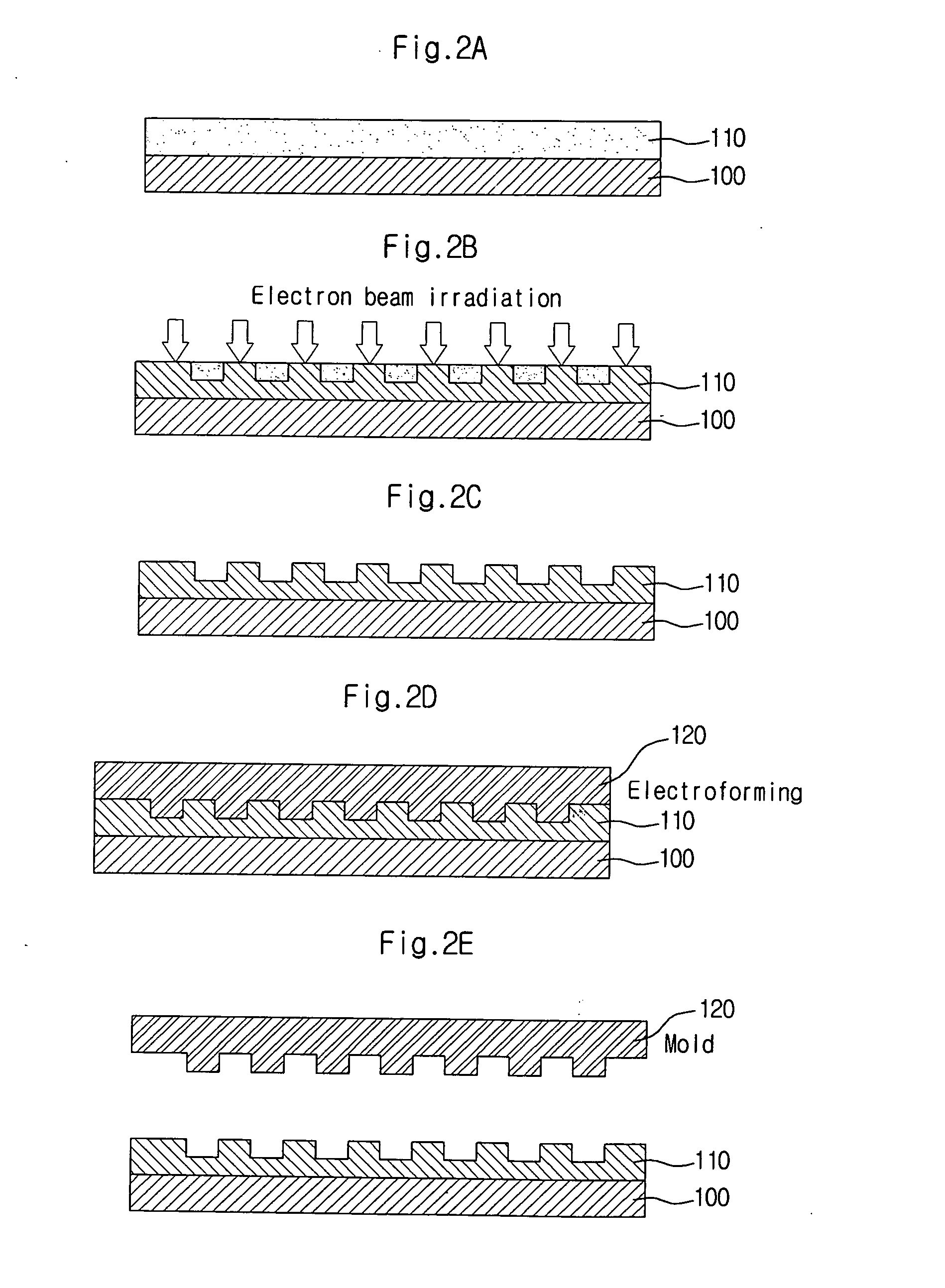
[0046]FIG. 2A to FIG. 2E diagrammatically illustrate one embodiment of a manufacturing procedure of a mold for use with the manufacture of a wavelength filter according to the present invention.

[0047] The mold has a concavo-convex shape opposite to the concavo-convex shape of a desired polymer fine pattern, and is preferably made from metallic materials with high strength, e.g., Nickel (Ni).

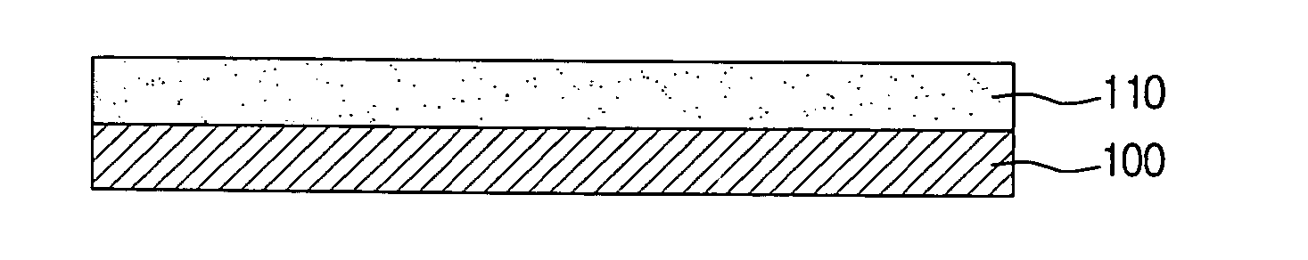
[0048] As shown in FIG. 2A, a polymer layer 110 is formed on a silicon substrate 100 by a spraying or spin coating method. In particular, the polymer layer 110 is deposited on the substrate 100 to a thickness of several micrometers.

[0049] As for the polymer layer 110 materials normally sensitive to electron beams such as PMMA (polymethylmethacrylate) are used.

[0050] Therefore, when the electron beams are irradiated over a certain part of the polymer layer, ...


PUM


Abstract

A manufacturing method of a wavelength filter includes the steps of: depositing on a substrate a lower clad layer and a core layer, each made from a polymer material; compressing the core layer with a mold to lithograph a pattern of the mold onto the core layer; stabilizing the lower clad layer and the core layer; separating the core layer from the mold; forming an upper clad layer on the core layer; and forming an electrode on the upper clad layer.

Description

BACKGROUND OF THE INVENTION [0001] 1. Field of the Invention [0002] The present invention relates to a manufacturing method of a wavelength filter for use with an optical Wavelength Division Multiplexing (WDM) communication system. [0003] 2. Discussion of the Background Art [0004] With the rapid increase of a variety of data including voice and image data, the world's attention has turned to studies about optical communication system for building a very high-speed broadband integrated communication network capable of integrating the data and transmitting and processing them at very high speed. [0005] In particular, an optical WDM communication system respectively inputs different information to many light sources with different wavelengths, and multiplexes them and transmits the multiplexed data through one single optical fiber. Then the receiving end thereof demultiplexes the multiplexed signal and receives optical signals according to their wavelengths. Therefore, the bandwidth of...

Claims


Application Information

Patent Timeline
IPC IPC(8): G02B6/12G02B6/124
CPCG02B6/124G02B6/12
Inventor AHN, SEH WONLEE, KI DONGLEE, SUNG EUN
Owner LG ELECTRONICS INC
Why Eureka
Try Eureka