
Semiconductor integrated circuit, method for driving semiconductor integrated circuit, method for driving electronic apparatus, display device, and electronic apparatus

a technology of semiconductor integrated circuits and integrated circuits, applied in the direction of electronic switching, pulse generators, pulse techniques, etc., can solve the problems of limiting the electrical field buffering effect based on the ldd structure, the residual defect density is high, and the maximum voltage applied to the respective transistors can be reduced, and the characteristics of the electronic apparatus can be improved. , the effect of favorable driving

Active Publication Date: 2010-07-29
SEIKO EPSON CORP
View PDF10 Cites 10 Cited by
  • Summary
  • Abstract
  • Description
  • Claims
  • Application Information

AI Technical Summary

Benefits of technology

[0012]Specifically, the electrical field buffering effect will become greater if the impurity concentration of the LDD structural part is set low, but the lower limit thereof is approximately several times the residual defect density of the layer that is used as the semiconductor layer (channel layer). In particular, a thin film transistor using low-temperature polysilicon has a high residual defect density at 1017 / cm2 or less, and the impurity concentration of the LDD structural part cannot be set low. Thus, there is a limit to the electrical field buffering effect based on the LDD structure.
[0069]According to the foregoing configuration, a display device can be manufactured easily and inexpensively.

Problems solved by technology

In particular, a thin film transistor using low-temperature polysilicon has a high residual defect density at 1017 / cm2 or less, and the impurity concentration of the LDD structural part cannot be set low.
Thus, there is a limit to the electrical field buffering effect based on the LDD structure.

Method used


Image

  • Semiconductor integrated circuit, method for driving semiconductor integrated circuit, method for driving electronic apparatus, display device, and electronic apparatus
  • Semiconductor integrated circuit, method for driving semiconductor integrated circuit, method for driving electronic apparatus, display device, and electronic apparatus
  • Semiconductor integrated circuit, method for driving semiconductor integrated circuit, method for driving electronic apparatus, display device, and electronic apparatus

Examples


first embodiment

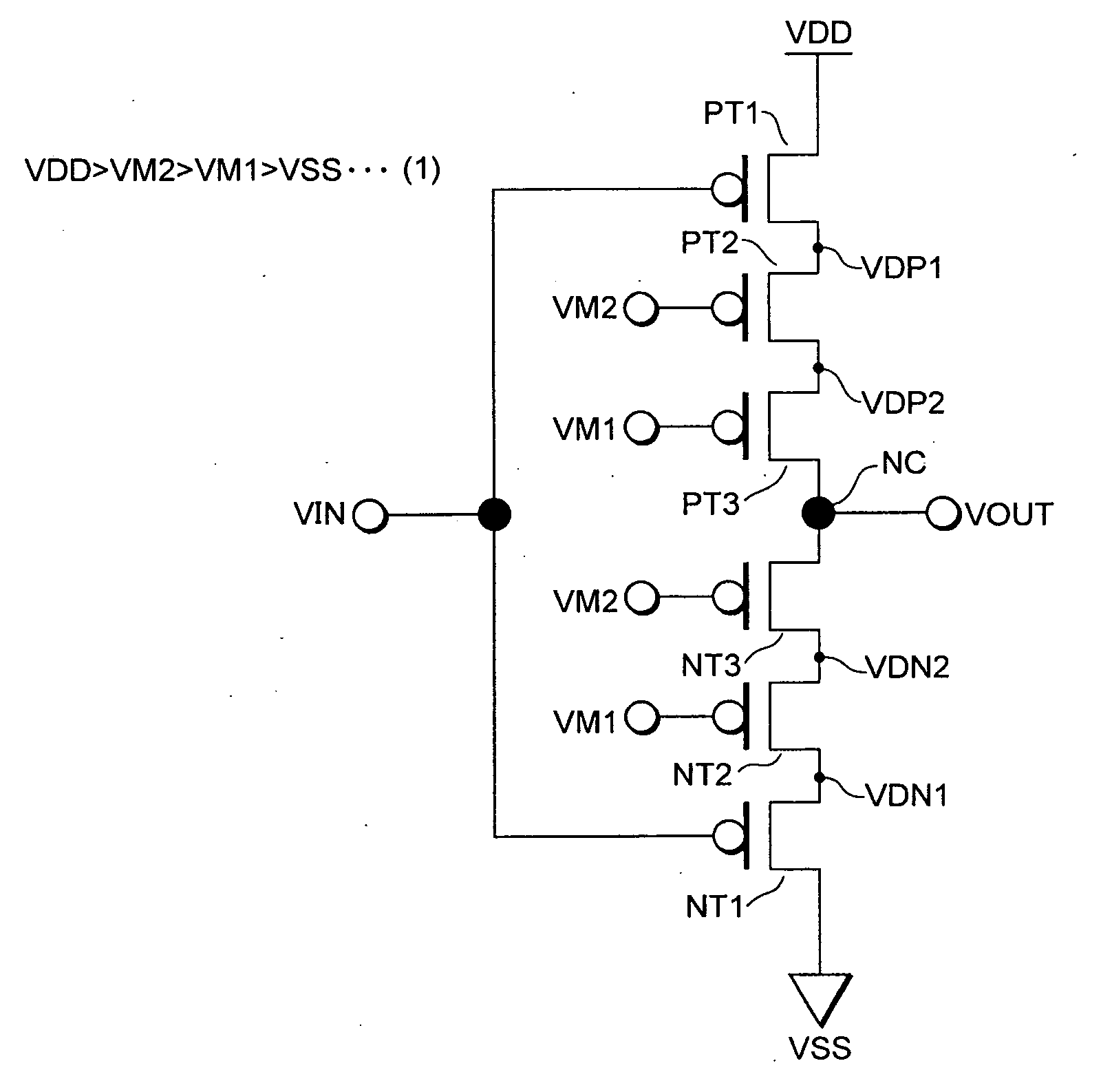
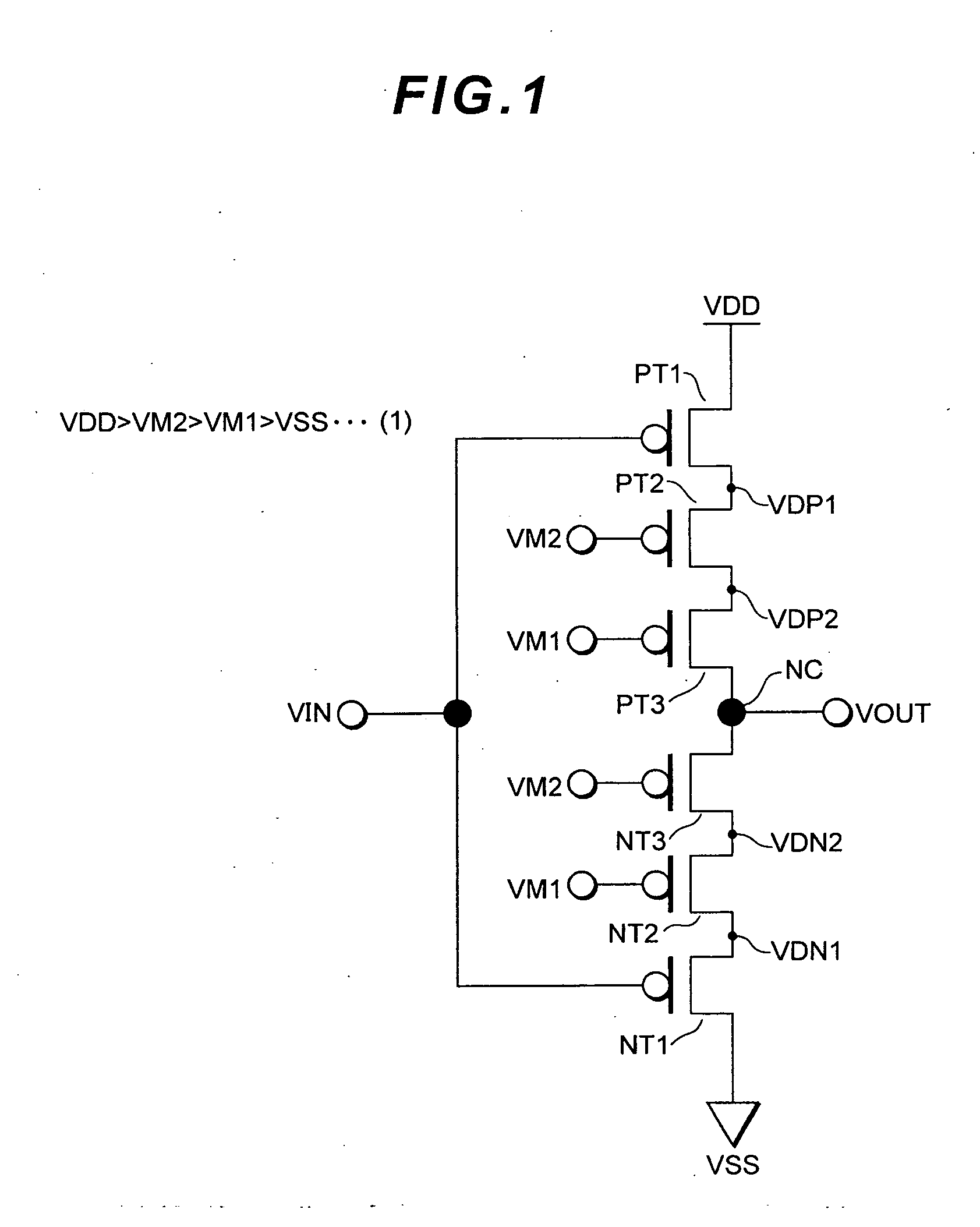
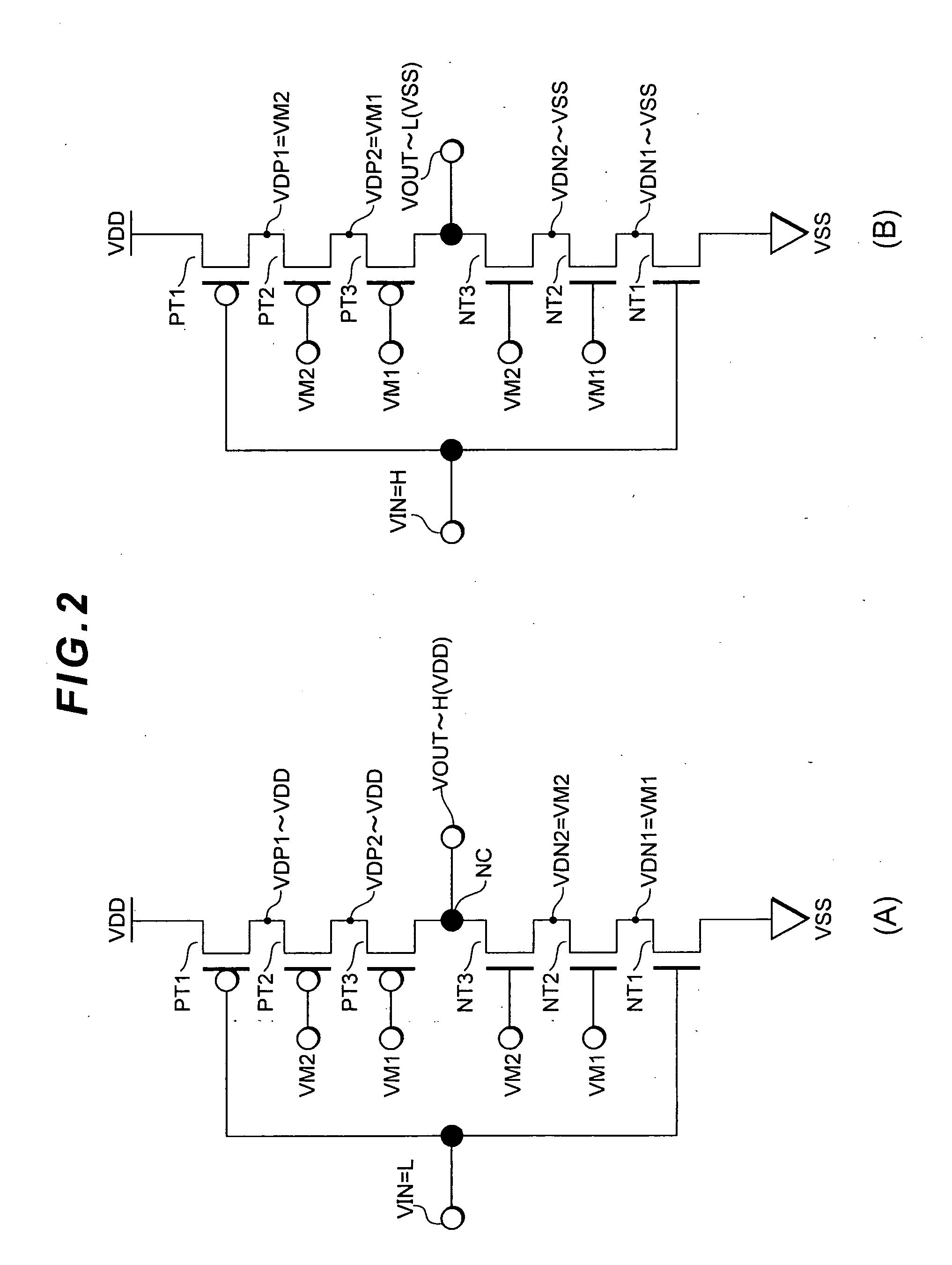
[0097]FIG. 1 is a circuit diagram showing the inverter circuit (semiconductor integrated circuit) of this embodiment, and FIG. 2A and FIG. 2B are diagrams showing the operation thereof. The inverter circuit of this embodiment is configured from a plurality of thin film transistors (TFT). In the ensuing explanation, a thin film transistor is simply referred to as a “transistor.” In this specification, a signal line, a node and their potential are given the same reference numeral.

[0098]A standard inverter circuit comprises a p-channel transistor (PT1) and an n-channel transistor (NT1) that are sequentially connected between a power source potential VDD and a grounding potential VSS, a gate terminal of these transistors is connected to an input signal line (input signal node) VIN, and a connection node NC of the p-channel transistor (PT1) and the n-channel transistor (NT1) is connected to an output signal line (output signal node) VOUT. In the ensuing explanation, these transistors (PT...

second embodiment

[0135]Although a voltage-dividing transistor was used in the inverter circuit in the first embodiment, an example of a level shifter circuit is explained in this embodiment.

[0136]FIG. 9 is a circuit diagram showing the level shifter circuit (semiconductor integrated circuit) of this embodiment, and FIG. 10A and FIG. 10B are diagrams showing the operation of the level shifter circuit of this embodiment.

[0137]A standard level shifter circuit comprises pairs of a p-channel transistor and an n-channel transistor (pairs of PT1 and NT1 and PT11 and NT11) that are connected in parallel between the second power source potential (high power source potential) VDD2 and the grounding potential VSS, and these connection nodes (NC1, NC2) are cross-connected to the p-channel transistors (PT1, PT11). The gate terminals of the n-channel transistors (NT1, NT11) are respectively connected to the input signal lines (input signal node) VIN+, VIN− to which a complemented signal is input. In addition, the...

third embodiment

[0158]Here, in the circuit diagram shown in FIG. 12, there are cases where the output voltage is not divided evenly and excessive voltage stress is applied to each P-channel transistor or N-channel transistor connected to the output voltage Vout if the input voltage is an intermediate level or the circuit is operated in a state where a high load is connected to the output side. This voltage stress induces deterioration in the performance of transistors, and diminishes the long-term reliability of the overall circuit.

[0159]As a comparative example explaining the foregoing problems, the following observation result is explained. After foremost explaining the circuit configuration, the basic I / O characteristics and the load characteristics will be explained subsequently.

[0160](1) Circuit Configuration

[0161]FIG. 12 is a circuit diagram showing the circuit configuration of the comparative example used in the observation. In FIG. 12, an inverter circuit is configured from two p-channel tr...


PUM


Abstract

The present invention provides a semiconductor integrated circuit capable of achieving high voltage. The proposed semiconductor integrated circuit includes a first node [VOUT] connected to a first potential node [VDD], and a first n-channel transistor [NT1] and a second n-channel transistor [NT2] serially connected between a first node [VOUT] and a second potential node [VSS] of a lower potential than the first potential node. One end of NT1 is connected to the second potential node [VSS], the other end thereof is connected to one end of the second n-channel transistor [NT2], a gate terminal thereof is connected to a second node [VIN], the other end of NT2 is connected to the first node [VOUT], and a gate terminal thereof is connected to a first intermediate range potential [VM1] positioned between the first potential node [VDD] and the second potential node [VSS].

Description

CROSS-REFERENCES TO RELATED APPLICATIONS[0001]This application relates to and claims priority from Japanese Patent Application No. 2008-314508, filed on Dec. 10, 2008, and from Japanese Patent Application No. 2009-075901, filed on Mar. 26, 2009, the entire disclosure of which is incorporated herein by reference.BACKGROUND[0002]1. Technical Field[0003]The present invention relates to a semiconductor integrated circuit, a method for driving a semiconductor integrated circuit, a method for driving an electronic apparatus, a display device, and an electronic apparatus.[0004]2. Related Art<First Background Art>[0005]A polysilicon thin film transistor (TFT) is used as a backplane of display devices such as a liquid crystal display device. For instance, a display unit (active matrix unit) or a drive circuit unit that is disposed at the periphery thereof is configured from a thin film transistor. A thin film transistor can be formed from a relatively low-temperature process, and is an...

Claims


Application Information

Patent Timeline
Patent Type & Authority Applications(United States)
IPC IPC(8): H01L27/088H01L25/00
CPCH01L27/12H03K19/00315H03K17/102H03K3/35613
Inventor IRIGUCHI, CHIHARU
Owner SEIKO EPSON CORP
Learn More