Optical module

a technology of optical modules and optical fibers, applied in the field of optical modules, can solve the problems of difficult to ensure the air tightness in the vicinity of optical fibers, easy to cause malfunctions, etc., and achieve the effects of reducing the size of modules, and enhancing the air tightness of optical systems

Active Publication Date: 2010-07-29
HAMAMATSU PHOTONICS KK
View PDF2 Cites 23 Cited by
  • Summary
  • Abstract
  • Description
  • Claims
  • Application Information

AI Technical Summary

Benefits of technology

[0007]The present invention has been achieved in consideration of the above-described problems, and an object of the present invention is to provide an optical module which is capable of enhancing the airtightness of an optical system including a movable mirror, and which can also be downsized.
[0008]In order to solve the above-described problems, there is provided an optical module according to the present invention, which is manufactured from a substrate product having a support substrate and a semiconductor layer disposed on one surface of the support substrate via an insulating layer, the optical module including a movable mirror which includes a portion of the semiconductor layer, and in which a mirror surface is formed on a side face intersecting with a predetermined direction, the movable mirror is movable in the predetermined direction along the one surface by eliminating the insulating layer between the portion of the semiconductor layer and the support substrate, an optical semiconductor element which is provided on the one surface of the support substrate, and is optically coupled to the mirror surface of the movable mirror, a cap member which is provided on the one surface of the support substrate, the cap member airtight-seals the movable mirror and the optical semiconductor element, and an element electrode part which is provided through the support substrate and the insulating layer, and is electrically connected to the optical semiconductor element.
[0009]In the optical module according to the present invention, the optical semiconductor element is provided on the support substrate, and the optical semiconductor element and the movable mirror are together airtight-sealed with the cap member. Then, the optical semiconductor element and the mirror surface of the movable mirror are optically coupled to one another. In accordance with such a configuration, there is no need to install an optical fiber for connecting to an external detector or the like as included in the device, that is disclosed in above-described Patent Document 1, and therefore, it is possible to enhance the airtightness of the optical system including the movable mirror with the cap member. Further, because the optical semiconductor element is provided on the support substrate, there is no need to provide a photodetector or the like outside the device, which makes it possible to downsize the module.
[0010]Further, in the case in which it is necessary to make electric connections with the structural members or electric elements on the support substrate, generally, a wiring pattern is formed on the support substrate, to be led out to the outside of the package of the module. However, the airtightness of the optical system including the movable mirror may be deteriorated due to the irregularity generated by such a wiring. There is also a method in which a place contacting the cap member is covered with an insulating film, and the insulating film is ground to flatten the contacting surface with the cap member, however, not only is the number of steps increased, but also, in some cases, it may be impossible to utilize such a method depending on a type of device. In contrast thereto, in the optical module according to the present invention, the element electrode part electrically connected to the optical semiconductor element is provided through the support substrate and the insulating layer. Thereby, it is possible to make an electric connection with the optical semiconductor element from above the other surface of the support substrate, and therefore, there is no need to lead out a wiring pattern on the one surface of the support substrate, and it is possible to further enhance the airtightness of the optical system including the movable mirror with the cap member.
[0011]In accordance with the above-described optical module, it is possible to enhance the airtightness of the optical system including the movable mirror, and to downsize the module.

Problems solved by technology

However, there are the following problems in the configuration described in Patent Document 1.
Further, because a driving part such as a movable mirror has a shape in dimensions from several μm to several tens of μm, that is minute, malfunction is easily caused therein due to dust, water droplets, and the like being adhered to a gap between the movable mirror and the substrate.
Accordingly, in order to prevent invasion of dust, water droplets, and the like, an optical system including a movable mirror is preferably airtight-sealed, however, in a configuration in which an output light such as an interference optical image is taken out via an optical fiber, it is difficult to sufficiently secure the airtightness in the vicinity of the optical fiber.

Method used


Image

  • Optical module
  • Optical module
  • Optical module

Examples


first embodiment

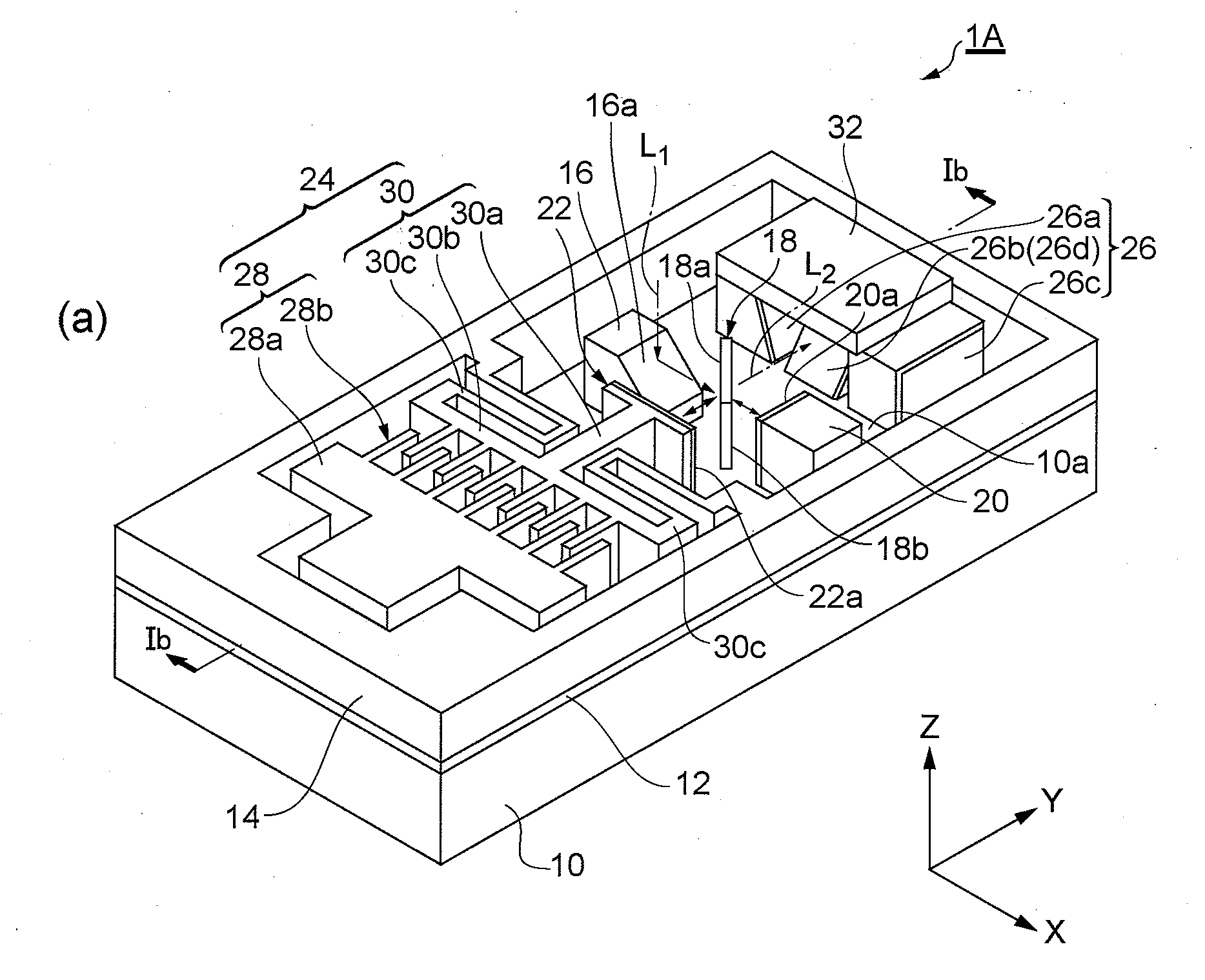
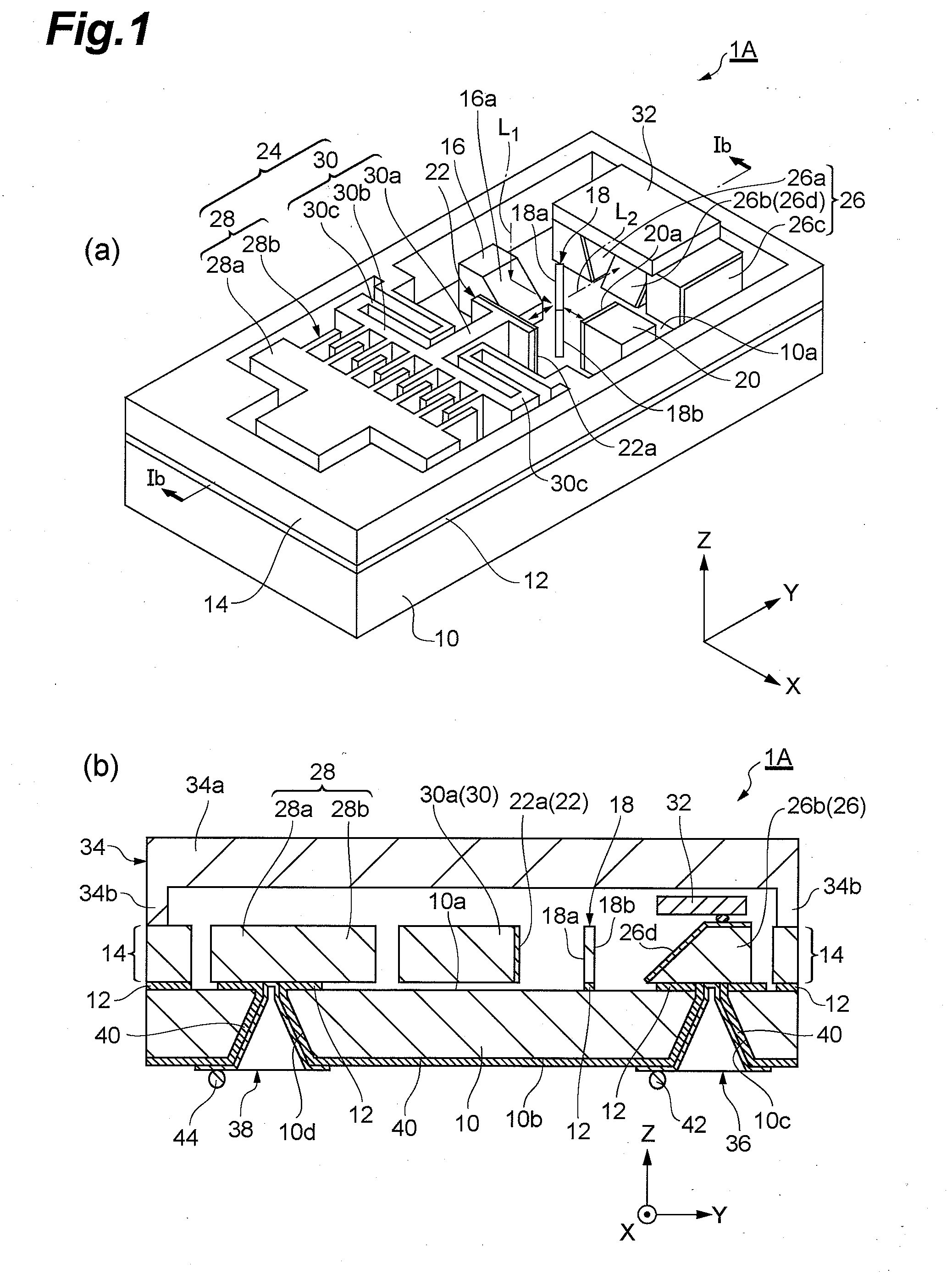
[0036]FIG. 1 shows diagrams showing a configuration of an optical module 1A as a first embodiment of an optical module according to the present invention. Here, (a) in FIG. 1 shows a perspective view of the optical module 1A, and (b) in FIG. 1 shows a sectional side view of the optical module 1A taken along the line Ib-Ib in FIG. 1(a). Note that, in FIG. 1(a), a cap member 34 included in the optical module 1A is omitted in the illustration to facilitate understanding thereof. Further, XYZ orthogonal coordinate systems are shown in FIG. 1(a) and FIG. 1(b).

[0037]The optical module 1A is manufactured from a substrate product such as an SOT substrate, and the optical module includes a support substrate 10 made of silicon (Si) having a pair of surfaces 10a and 10b, an insulating layer 12 provided on the one surface 10a of the support substrate 10, and a conductive semiconductor layer 14 disposed on the surface 10a of the support substrate 10 via the insulating layer 12. The insulating la...

second embodiment

[0084]FIG. 21 shows diagrams showing a configuration of an optical module 1B as a second embodiment of an optical module according to the present invention. Here, (a) in FIG. 21 shows a plan view of the optical module 1B, and (b) in FIG. 21 shows a sectional side view of the optical module 1B taken along the line XXIb-XXIb in FIG. 21(a). Note that, in FIG. 21(a), the cap member 34 included in the optical module 1B is omitted in the illustration to facilitate understanding thereof. Further, XYZ orthogonal coordinate systems are shown in FIG. 21(a) and FIG. 21(b).

[0085]The optical module 1B of the present embodiment is manufactured from an SOI substrate in the same way as the optical module 1A of the first embodiment, and the optical module includes the support substrate 10, the insulating layer 12, and the semiconductor layer 14. Further, the movable mirror 22 and the electrostatic actuator 24 as parts of the structural members for constituting a Michelson interference optical system...


PUM


Abstract

An optical module 1A is an optical module, which is manufactured from an SOI substrate having a support substrate 10 and a semiconductor layer 14 disposed on a surface 10a of the support substrate 10 via an insulating layer 12, the optical module including a movable mirror 22 in which a mirror surface 22a is formed on a side face intersecting with a Y-direction, that is movable in the Y-direction, a photodiode 32 which is provided on the surface 10a of the support substrate 10, and is optically coupled to the mirror surface 22a of the movable mirror 22, a cap member 34 which is provided on the surface 10a of the support substrate 10, that airtight-seals the movable mirror 22 and the photodiode 32, and an element electrode part 36 which is provided through the support substrate 10 and the insulating layer 12, and is electrically connected to the photodiode 32. Thereby, it is possible to realize an optical module which is capable of enhancing the airtightness of an optical system including a movable mirror, and which also can be downsized.

Description

CROSS-REFERENCE TO RELATED APPLICATION[0001]This application claims priority to Provisional Application Ser. No. 61 / 147,230 filed on Jan. 26, 2009, which is hereby incorporated by reference in its entirety.BACKGROUND OF THE INVENTION[0002]1. Field of the Invention[0003]The present invention relates to an optical module using a MEMS (Micro Electro Mechanical Systems) technology.[0004]2. Related Background Art[0005]In recent years, the development of MEMS devices manufactured by use of the MEMS technology has been advanced, and such MEMS devices can be put into practice as various optical components. For example, in Patent Document 1, there is disclosed an interference optical system which is configured on an SOI (Silicon On Insulator) substrate by use of the MEMS technology. The interference optical system according to Patent Document 1 includes a beam splitter, a movable mirror attached to an electrostatic actuator, and a fixed mirror, and these are formed by applying etching to a s...

Claims


Application Information

Patent Timeline
Patent Type & Authority Applications(United States)
IPC IPC(8): G02B26/00
CPCB81B7/0067G01B9/02B81B2207/096B81B2201/042G01B9/02051
Inventor WARASHINA, YOSHIHISASUZUKI, TOMOFUMI
Owner HAMAMATSU PHOTONICS KK
Why Eureka
Try Eureka