Target and method for mask-to-wafer cd, pattern placement and overlay measurement and control

a mask-to-wafer and pattern-to-wafer technology, applied in the field of integrated circuit manufacturing, can solve the problems of limited application of current technology, prone to chemical mechanical planarization, thermal processing, etc., and achieve the effect of reducing the critical dimension and the variation of the overlay

Inactive Publication Date: 2010-07-29
GLOBALFOUNDRIES INC
View PDF4 Cites 25 Cited by
  • Summary
  • Abstract
  • Description
  • Claims
  • Application Information

AI Technical Summary

Benefits of technology

[0006]Bearing in mind the problems and deficiencies of the prior art, it is therefore an object of the present invention to provide an improved target and method for determination of overlay error within a chip level.
[0007]It is another object of the present invention to provide an improved target and method for correlating mask-to-wafer variations of critical dimension and overlay.
[0008]A further object of the invention is to provide an improved target and method for distinguishing mask and wafer components of critical dimension and overlay variation.
[0009]It is yet another object of the present invention to provide an improved target and method to minimize on-wafer critical dimension and overlay variation.
[0010]It is another object of the present invention to provide an improved target and method that measures mask and wafer registration, critical dimension at the same physical location.
[0013]The method preferably further includes using the correlated mask and wafer measurements to control the mask and wafer fabrication processes to minimize wafer critical dimension and overlay variation.

Problems solved by technology

Current technology has limited application due to size restriction for placement around the mask reticle field.
Hence, these targets are susceptible to chemical mechanical planarization, thermal processing, and lithography image processing.

Method used


Image

  • Target and method for mask-to-wafer cd, pattern placement and overlay measurement and control
  • Target and method for mask-to-wafer cd, pattern placement and overlay measurement and control
  • Target and method for mask-to-wafer cd, pattern placement and overlay measurement and control

Examples


Embodiment Construction

)

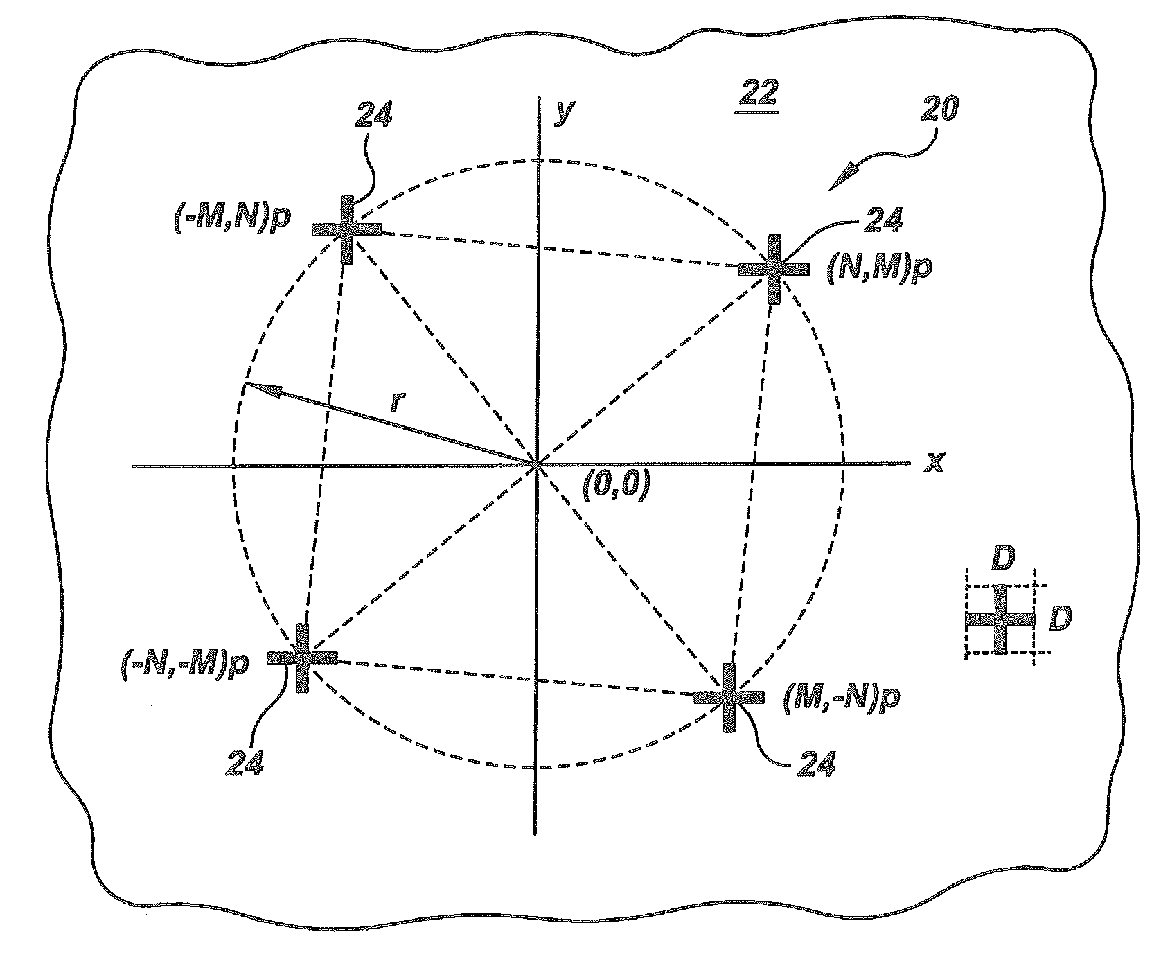
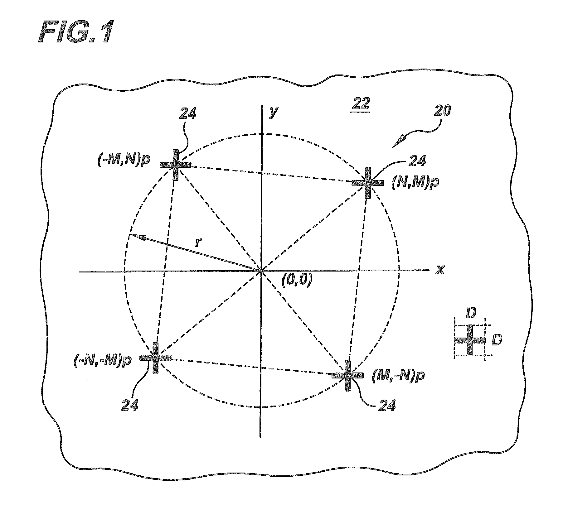
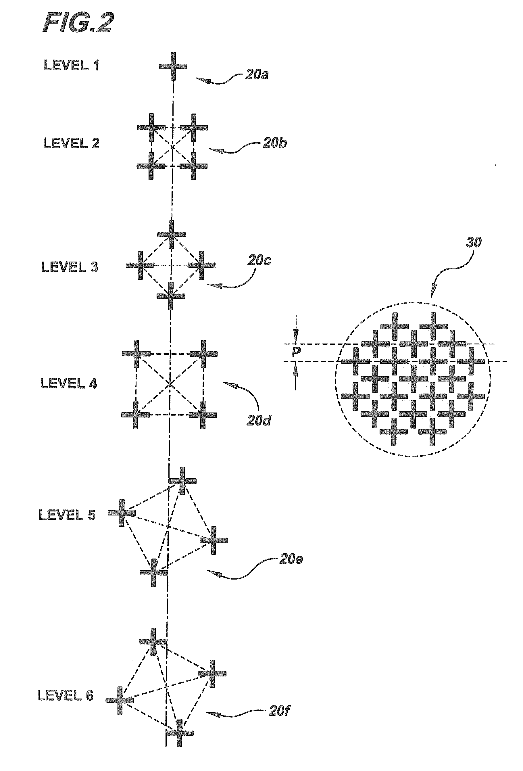
[0044]In describing the preferred embodiment of the present invention, reference will be made herein to FIGS. 1-12 of the drawings in which like numerals refer to like features of the invention.

[0045]The present invention provides a target and method for combining both reticle critical dimension (CD) and registration measurement with wafer level or layer overlay measurement in the lithographic production of integrated circuits. The invention allows for precise correlation of wafer level or layer overlay measurements and reticle registration measurements, as well as vastly improving the ability to make thru-field overlay measurements. The invention also provides a method for separating reticle-induced overlay components from wafer exposure-induced overlay errors. This is particularly important because double exposure patterning, where a mask prints first set of lines and then shifts to print a second set of lines, is often used because there is not sufficient resolution to print req...


PUM

PropertyMeasurementUnit
circuit structureaaaaaaaaaa
critical dimensionaaaaaaaaaa
optical microscopyaaaaaaaaaa

Abstract

A method for mask-to-wafer correlation among multiple masking levels of a semiconductor manufacturing process. The method includes creating compact targets containing structure patterns suitable for pattern placement, critical dimension and overlay measurement at a set of common locations on two or more patterning layers, and creating at least two masks containing functional circuit structure patterns and the compact targets at locations between functional circuit structure patterns. The method then includes measuring the targets, determining overlay variation between the masks, exposing and creating with one mask a first lithographic processing layer on a wafer, and exposing and creating with another mask a second lithographic processing layer on the wafer, over the first layer. The method further includes measuring the targets on the wafer at one or more of the layers, and correlating the mask and wafer measurements to distinguish mask and lithography induced components of critical dimension and overlay variation.

Description

BACKGROUND OF THE INVENTION[0001]1. Field of the Invention[0002]The present invention relates to the manufacture of integrated circuits by a lithographic process and, in particular, to a method and system for determining critical dimension or overlay variation of integrated circuit fields within and between chip levels and layers.[0003]2. Description of Related Art[0004]Semiconductor integrated circuit manufacturing requires the sequential patterning of process levels on a single semiconductor wafer. Exposure tools print multiple integrated circuit patterns or fields by lithographic methods on successive levels of the wafer. These tools typically pattern the different levels by applying step and repeat lithographic exposure or step and scan lithographic exposure in which the full area of the wafer is patterned by sequential exposure of the stepper fields containing one or more integrated circuits. Typically, 20-50 levels are required to create an integrated circuit. In some cases, m...

Claims


Application Information

Patent Timeline
Patent Type & Authority Applications(United States)
IPC IPC(8): G03F1/00G06F7/20
CPCG03F1/14G03F1/144G03F7/70683G03F7/70625G03F7/70633G03F1/42G03F1/00G03F1/68G03F1/62H01L21/0274G03F1/36
Inventor AUSSCHNITT, CHRISTOPHER P.MORILLO, JAIME D.RANKIN, JED H.YERDON, ROGER J.
Owner GLOBALFOUNDRIES INC
Why Eureka
Try Eureka