

Device for polishing the edge of a semiconductor substrate
a technology for polishing devices and semiconductor substrates, applied in edge grinding machines, manufacturing tools, lapping machines, etc., can solve problems such as deformation of planarity
- Summary
- Abstract
- Description
- Claims
- Application Information
AI Technical Summary
Benefits of technology
Problems solved by technology
Method used
Image

Examples
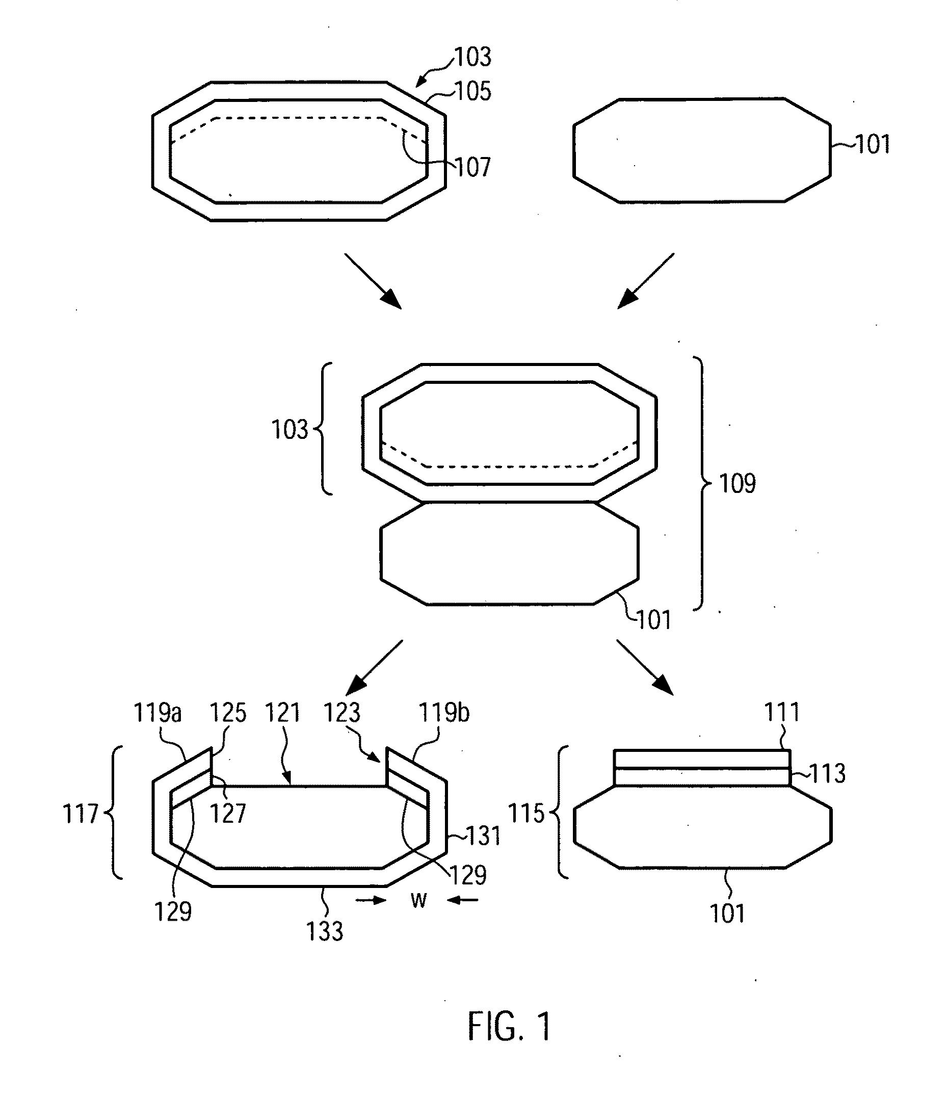
first embodiment
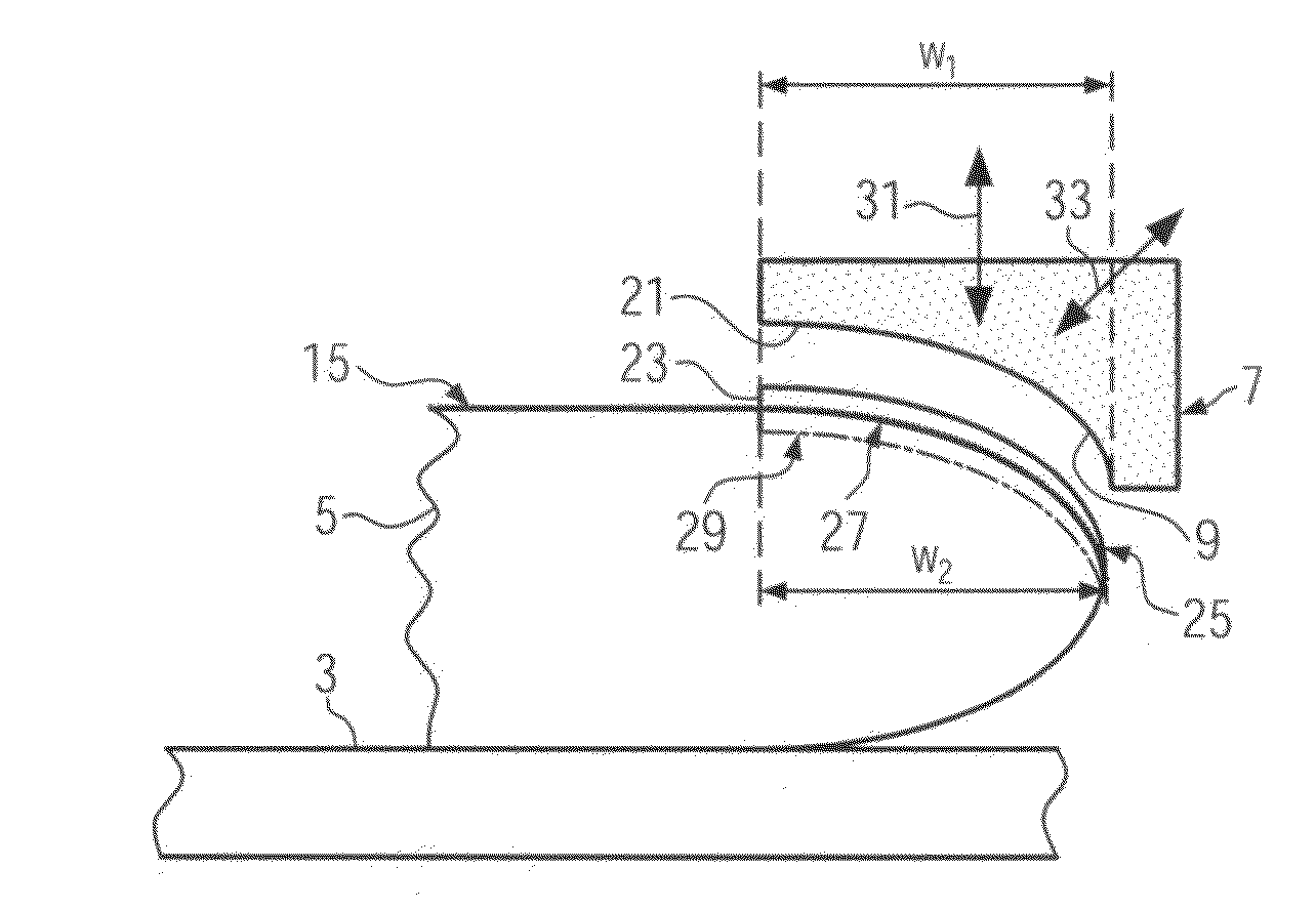
[0043]FIG. 3 illustrates pad holder 7 and polishing pad 9 according to the invention. Here both elements are illustrated as one unit. The cross sectional view illustrated in FIG. 3 is the same as the one illustrated in FIG. 2.
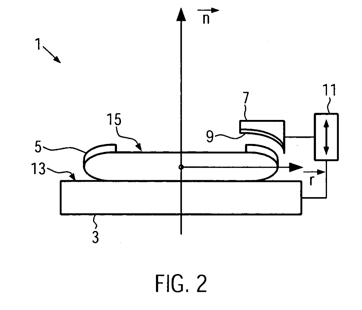
[0044]The cross section of pad holder 7 / polishing pad 9 has a concave shaped part 21 facing the substrate 5 positioned on the substrate holder 3. In the lateral direction, thus in the radial direction r in FIG. 2 of substrate 5, the pad holder 7 / polishing pad 9 has its concave portion 21 extending over at least a width w1 corresponding to the width w2 of the edge portion of substrate 5 that carries the protruding residual topography 23 (see also FIG. 1). Typically, the width w2 is of the order of 1.5 mm so that w1 is also of at least 1.5 mm.
[0045]According to the variant, the width w1 is chosen to be at least 3 mm. In this case it becomes possible to remove also the protruding topography in the notch region of a semiconductor wafer.
[0046]The concave shape 21 of...
third embodiment
[0052]FIG. 5 illustrates the pad holder 7″ and polishing pad 9″. The shape of the cross section facing the substrate 5 positioned on substrate holder 3 has a plane part 51 positioned between two convex parts 53, 55. This shape is specially adapted to remove the step 23 in the edge region of substrate 5, in particular when it is associated with a vertical movement along arrow 57 controlled by control unit 11, which is illustrated in FIG. 2. This embodiment has the advantage that it is easy to realize. It can be associated with an additional edge polishing step to remove the unwanted parts positioned above the predetermined splitting area 27 on the side of substrate 5.
fourth embodiment
[0053]FIG. 6 illustrates a pad holder 7′″ and polishing pad 9′″ which combines a central concave portion 61 and two convex portions 63, 65 and the side facing the surface 15 of the substrate 5. In this embodiment, with one translational direction along arrow 67 or 69, thus along a vertical direction or an oblique direction, the desired final shape of substrate 5 can be achieved with one polishing step, in particular also on the side 25 of substrate 5, so that an additional edge polishing step becomes obsolete. Furthermore, due to the smooth transition between the concave and convex portions, the transition between the area with the step 23 and the area on the surface of substrate 5 without step 15 (where detachment occurred), is also smooth.
[0054]All embodiments of the invention have the advantage that the undesired protruding residual topography in the peripheral region of the substrate can be completely removed. As a consequence a double-sided polishing, like in the prior art, is ...
PUM
| Property | Measurement | Unit |
|---|---|---|
| Length | aaaaa | aaaaa |
| Length | aaaaa | aaaaa |
| Shape | aaaaa | aaaaa |
Abstract
Description
Claims
Application Information