Solder material, method for manufacturing the same, joined body, method for manufacturing the same, power semiconductor module, and method for manufacturing the same

a technology of solder material and manufacturing method, which is applied in the direction of manufacturing tools, soldering devices, and capacitors, can solve the problems of high cost and difficult application to consumer devices, and achieve the effect of improving the wetness of solder

Inactive Publication Date: 2010-08-05
TOYOTA JIDOSHA KK +1
View PDF6 Cites 33 Cited by
  • Summary
  • Abstract
  • Description
  • Claims
  • Application Information

AI Technical Summary

Benefits of technology

[0112]According to the present invention described in the twenty-sixth aspect, the members can be densely joined together, the wettability of the solder is improved, and deficiencies, such as joining of joined members at an angle, are unlikely to occur.
[0113]Further, according to the present invention described in the twenty-sixth aspect, the metal surface layer arranged on the nickel layer can be eliminated by heating during joining, without separately arranging a process therefor.

Problems solved by technology

However, lead is poisonous and is thus there is a trend towards the abolition of its use, and there have been demands for development of lead-free solder materials.
There are examples where an Au—Sn alloy (having a melting point of 280° C.) has been used for specific applications, but this alloy is a material containing 80% Au and is thus very expensive and difficult to apply to consumer devices.
As one type of harmless joining material having a melting point higher than 250° C., an Ag based brazing material is generally known, but this material has a high melting point of 600° C. or more such that, when it is used in joining by melting at such a temperature, it damages and denatures semiconductor elements, thus making it unusable for the present purpose.

Method used


Image

  • Solder material, method for manufacturing the same, joined body, method for manufacturing the same, power semiconductor module, and method for manufacturing the same
  • Solder material, method for manufacturing the same, joined body, method for manufacturing the same, power semiconductor module, and method for manufacturing the same
  • Solder material, method for manufacturing the same, joined body, method for manufacturing the same, power semiconductor module, and method for manufacturing the same

Examples


example 1

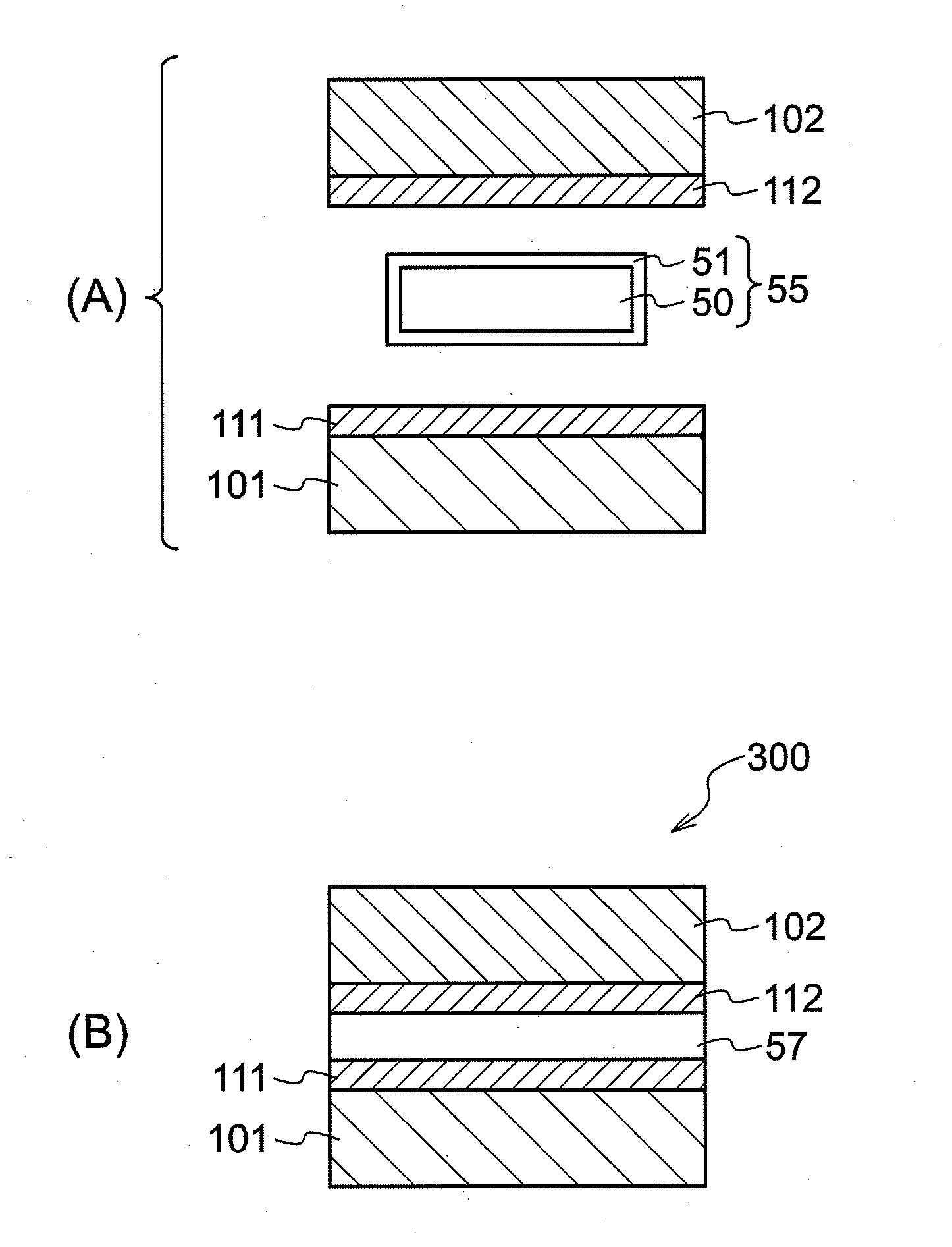
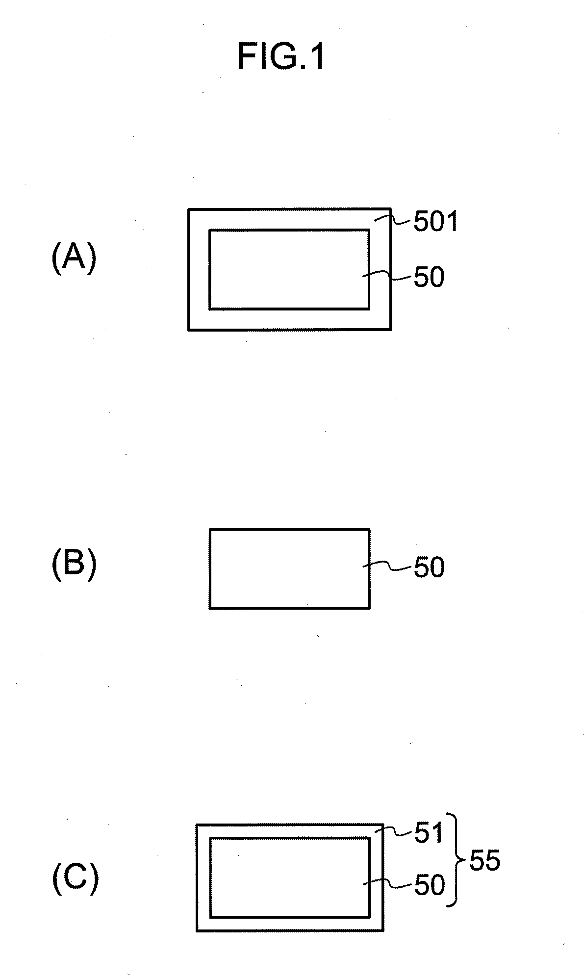
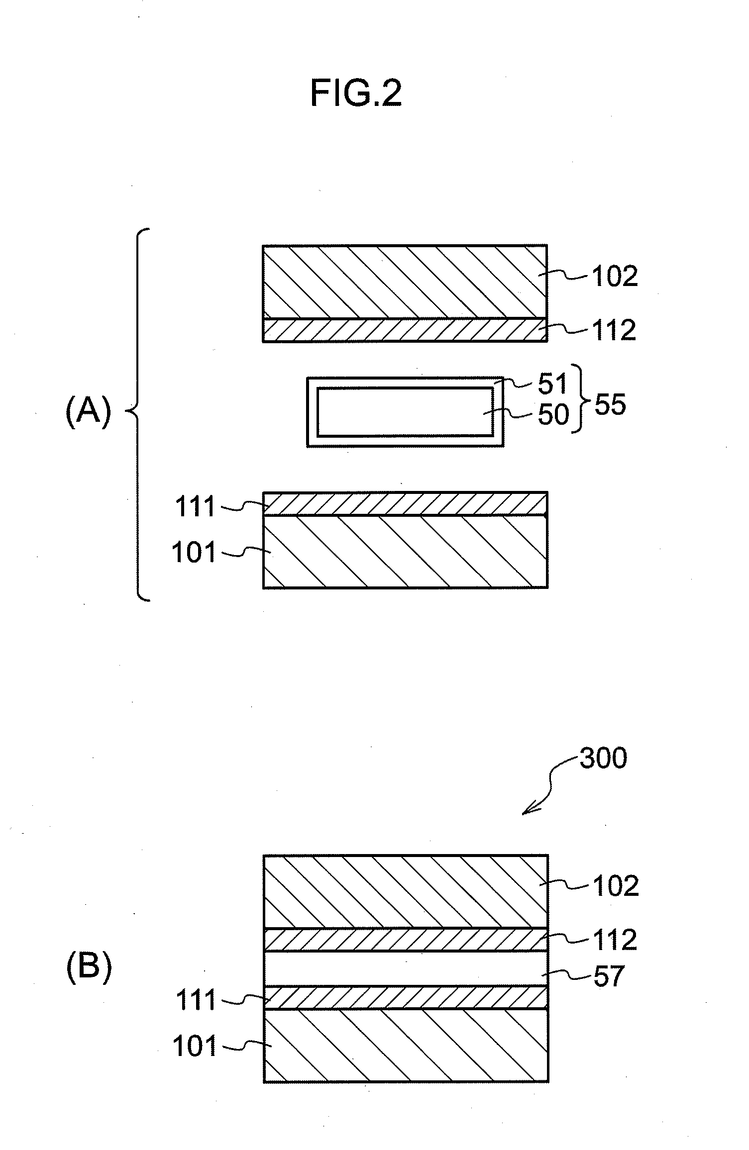
[0303]According to FIG. 7 (A) (B), a power semiconductor element and an insulating substrate were joined together with a Zn based solder material 55 to prepare an evaluation test specimen-1 having the structure shown in FIG. 7 (B).

[0304]

[0305]A power semiconductor element 20 using GaN was prepared, and on the outermost surface of the element, a Ni layer 22 was formed by sputtering. On the surface of the Ni layer 22, an Au layer (not shown in the figure) was formed by sputtering.

[0306]

[0307]Separately, Cu layers 34 and 36 were stuck by brazing onto both sides of a Si3N4 ceramic plate as an insulating substrate 32 to prepare a layered body of Cu layer 34 / Si3N4 layer 32 / Cu layer 36. A Ni layer 38 was formed by plating on the surface of the Cu layer in this layered body to prepare an insulating portion 30. In this plating, a surface not to be plated was protected with a masking sheet or the like.

[0308]

[0309]A solder material including 4% by mass of Al added to zinc (Zn0.96Al0.04 alloy: ...

example 2

[0322]In Example 2, removal of the natural oxide film and subsequent formation of the copper film were conducted by plating, replacing of bias sputtering and sputtering in Example 1.

[0323]A solder material including 4% by mass of Al added to zinc (Zn0.96Al0.04 alloy: melting point 380° C.) was prepared and processed by rolling into a foil of 0.1 mm in thickness. Then, the solder foil was placed in a pretreatment liquid for removing an oxide film, and then dipped in a copper plating liquid. Based on the previously determined relationship between plating thickness and plating time, the plating conditions were regulated such that the plating thickness reached 50 nm.

[0324]After plating, the specimen was used to prepare a joined body in the same manner as in Example 1 to give an evaluation test specimen-3.

[0325]The joined surface of the evaluation test specimen-3 thus obtained was observed in the same manner as in Example 1. As a result, at the joined surface of the evaluation test speci...

example 3

[0326]According to FIG. 8(A) (B), a power semiconductor element and an insulating substrate were joined together with a Zn based solder material 55 to prepare an evaluation test specimen-4 having the structure shown in FIG. 8 (B).

[0327]

[0328]A GaN power semiconductor element 20 having 1 cm2 of a surface to be joined was prepared, and on the outermost surface of the element, a Ni layer 22 was formed by sputtering. On the surface of the Ni layer 22, a Cu layer 24 was formed by sputtering. The thickness of the Ni layer 22 was 0.7 μm, and the thickness of the Cu layer 24 was 50 nm by measurement under an electron microscope.

[0329]

[0330]Meanwhile, Cu layers 34 and 36 were stuck by brazing onto both sides of a Si3N4 ceramic plate as an insulating substrate 32 to prepare a layered body of Cu layer 34 / Si3N4 layer 32 / Cu layer 36.

[0331]A Ni layer 38 was formed by plating on the surface of the Cu layer in the layered body, and a Cu layer 39 was formed by sputtering on the Ni layer 38, to prepa...


PUM

PropertyMeasurementUnit
thicknessaaaaaaaaaa
thicknessaaaaaaaaaa
thicknessaaaaaaaaaa

Abstract

A zinc based solder material 55 of the present invention is prepared by providing on the surface of a zinc based material 50, from which an oxide film 501 has been removed or at which an oxide film 501 does not exist, with a coating layer 51 containing primarily a metal whose oxide is more easily reducible than the oxide film 501. In a joined body and a power semiconductor module of the present invention, the zinc based solder material 55 is used in the joining portion, and after joining, the coating layer 51 does not exist.

Description

TECHNICAL FIELD[0001]The present invention relates to a solder material and a method for manufacturing the same, a joined body and a method for manufacturing the same, and a power semiconductor module and a method for manufacturing the same. The invention relates in particular to a lead-free solder material, a joined body and a power semiconductor module using a lead-free solder material, and a method for manufacturing them.BACKGROUND ART[0002]Up to now, lead (Pb) based solder materials have been used widely as solder materials. Particularly, Pb—Sn solder materials have been used in which their melting point is changed in the range of from about 183 to about 300° C. by changing the ratio of lead (Pb) to tin (Sn) therein, whereby solder materials having a suitable soldering temperature have been obtained (see for example, Non-Patent Document 1).[0003]However, lead is poisonous and is thus there is a trend towards the abolition of its use, and there have been demands for development o...

Claims


Application Information

Patent Timeline
Patent Type & Authority Applications(United States)
IPC IPC(8): H01L23/488H01L21/60H01L29/12H01B5/00B23K35/14B23K1/20B05D3/00
CPCB23K35/282B23K35/40C22C18/04H01L24/29H01L24/32H01L24/83H01L2224/27013H01L2224/32014H01L2224/83051H01L2224/83101H01L2224/83801H01L2924/01004H01L2924/01005H01L2924/01012H01L2924/01013H01L2924/01015H01L2924/01018H01L2924/01025H01L2924/01029H01L2924/0103H01L2924/01032H01L2924/01033H01L2924/01042H01L2924/01046H01L2924/01047H01L2924/0105H01L2924/01051H01L2924/01074H01L2924/01078H01L2924/01079H01L2924/01082H01L2924/01322H01L2924/19042H01L2924/0132H01L2224/29H01L2224/29298H01L2924/01006H01L2924/01019H01L2924/014H01L2224/29101H01L2924/0135H01L2924/0134H01L2924/1579H01L2224/29111H01L2224/29118H01L2924/00013H01L2224/26175H01L2224/291Y10T428/12222H01L2924/00H01L2924/01049H01L2924/01028H01L2924/3512H01L2924/00015H01L2924/00014H01L2224/29099H01L2224/29199H01L2224/29299H01L2224/2929H01L2924/00011H01L2924/351H01L2224/83205
Inventor YAMADA, YASUSHIYAGI, YUJITAKAKU, YOSHIKAZUOHNUMA, IKUOISHIDA, KIYOHITOATSUMI, TAKASHINAKAGAWA, IKUOSHIRAI, MIKIO
Owner TOYOTA JIDOSHA KK
Why Eureka
Try Eureka