Liner materials and related processes for 3-d integration

a technology of liner materials and integrated circuits, applied in the direction of semiconductor devices, semiconductor/solid-state device details, electrical devices, etc., can solve the problems of increasing speed related problems, reducing the performance of the system, and reducing the efficiency of the system,

Active Publication Date: 2010-08-12
ASM INTERNATIONAL
View PDF51 Cites 22 Cited by
  • Summary
  • Abstract
  • Description
  • Claims
  • Application Information

AI Technical Summary

Benefits of technology

[0008]The present application provides methods and devices related to the deposition of a liner material, preferably a low-k film liner material such as a polymerizable organo-silicon compound such as a benzocyclobutene compound, using a chemical vapor deposition (CVD) process, on sidewalls of a through-silicon via. In some embodiments, a method of forming an integrated circuit device comprises providing a first semiconductor workpiece and forming one or more vias in the first semiconductor workpiece. The vias are lined with a benzocyclobutene film. Conductive material is d...

Problems solved by technology
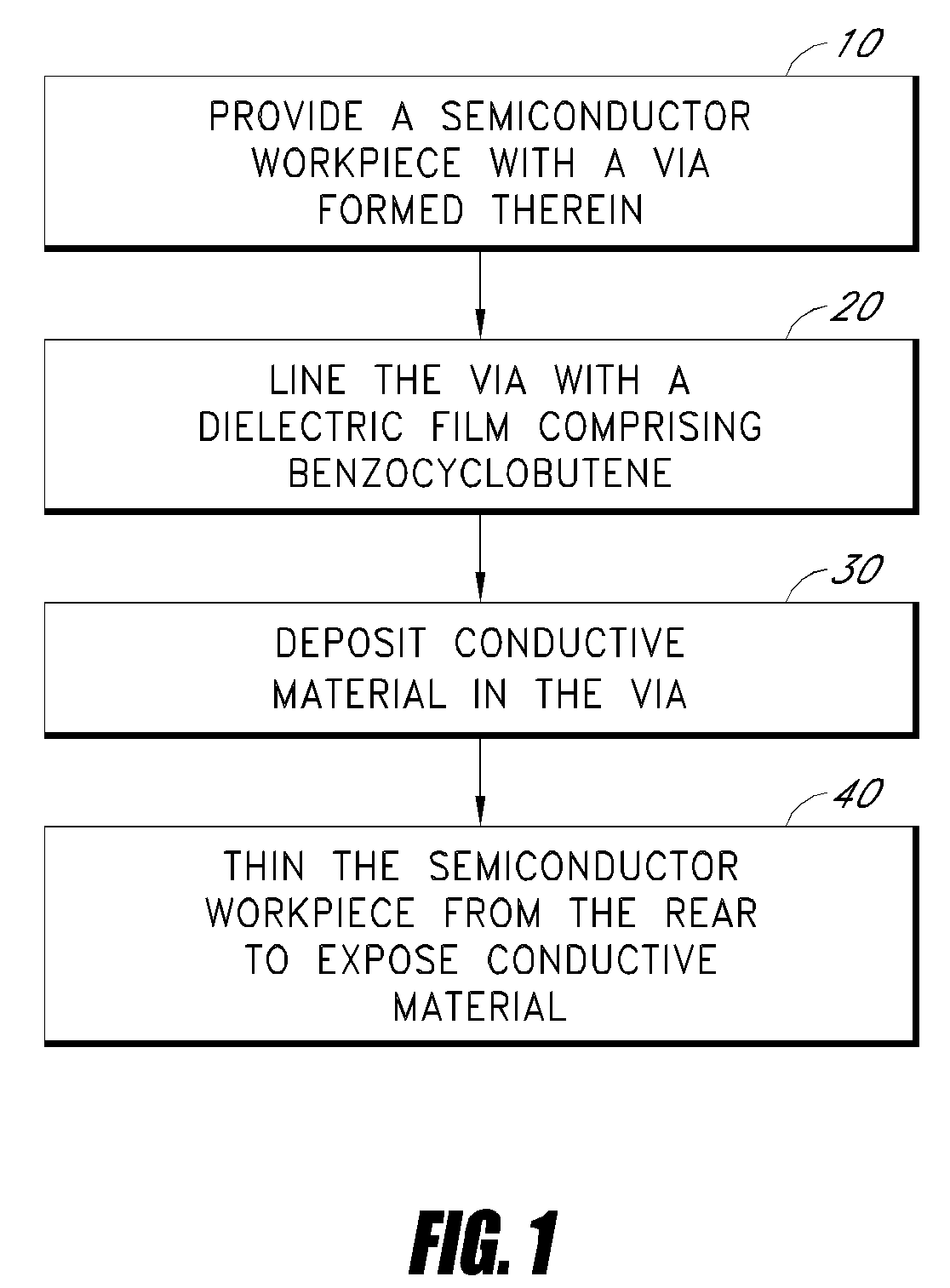
However, as more complex ICs such as microprocessors having high operating frequency ranges are manufactured, various speed related problems are becoming increasingly challengin...

Method used


Image

  • Liner materials and related processes for 3-d integration
  • Liner materials and related processes for 3-d integration
  • Liner materials and related processes for 3-d integration

Examples


example a

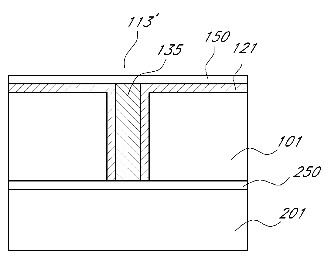
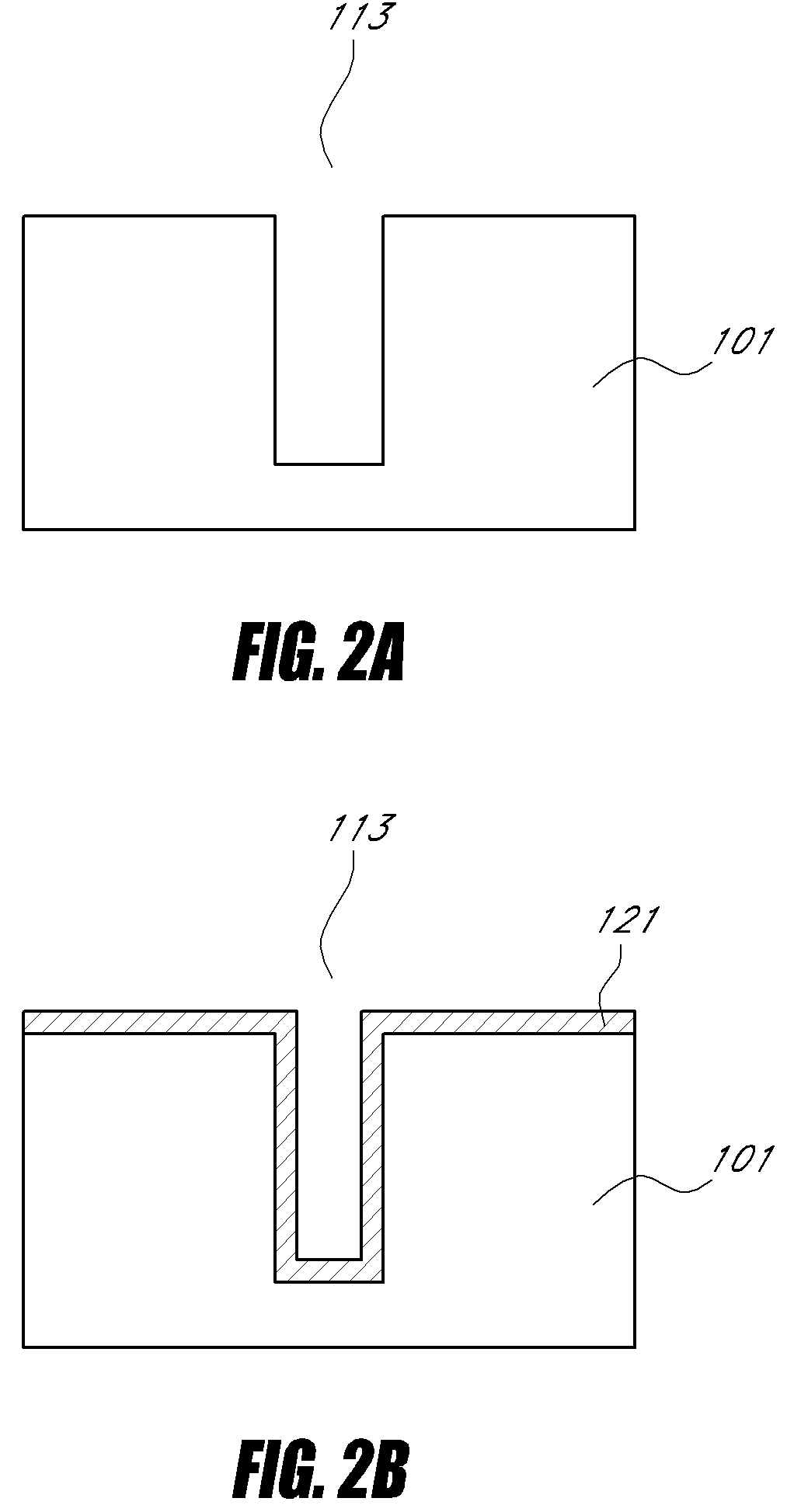
[0045]A first semiconductor workpiece is provided in an Eagle® 10 chemical vapor deposition chamber, commercially available from ASM Japan K.K. of Tokyo. A via or opening is provided in the workpiece. The via, which is subsequently formed into a through-silicon via, has a width of between 1 and 5 microns and a depth much greater, between 10 and 50 microns.

[0046]A first benzocyclobutene film is deposited on the via using a plasma enhanced chemical vapor deposition process. The deposition of the first benzocyclobutene film takes place at a temperature between about 200° C. and about 450° C. and a pressure between about 150 and about 600 Pa. The benzocyclobutene film is introduced at a mass flow rate of between about 0.1 g / min and about 0.2 g / min. The benzocyclobutene is introduced with a carrier gas comprising He, which has a flow rate between about 300 and about 800 sccm. To generate plasma, a high RF power of between about 50 and about 300 W and a high RF frequency between about 13....


PUM


Abstract

In some embodiments, a low-k dielectric film liner, preferably comprising benzocyclobutene, is deposited on the sidewalls of through-silicon vias used in three-dimensional (3-D) integration of integrated circuits. A semiconductor workpiece having a via is provided. A dielectric film liner, preferably comprising benzocyclobutene, is deposited on the sidewalls of the via by chemical vapor deposition. Following the deposition of the dielectric film liner, conductive material is deposited into the via. The conductive material on the bottom of the via can be exposed by thinning the back of the semiconductor workpiece, thereby forming a through-silicon via. The semiconductor workpiece can form a stack with one or more additional semiconductor workpieces having vias filled with conductive material to form a 3-D integrated circuit. The conductive material electrically interconnects the integrated circuits at different levels of the stack.

Description

BACKGROUND[0001]1. Field of the Invention[0002]This application relates generally to integration circuit fabrication. More particularly, this application relates to the deposition of liners for through-silicon vias used in the 3-D integration of integrated circuits.[0003]2. Description of the Related Art[0004]Integrated circuits (ICs) typically include many devices and circuit features formed on a single semiconductor wafer. Current trends in IC technology are toward faster and more powerful circuits. However, as more complex ICs such as microprocessors having high operating frequency ranges are manufactured, various speed related problems are becoming increasingly challenging. This is especially true when ICs having different functions are used to create electronic systems, for example, computing systems including processor and memory ICs, where different ICs are electrically connected by a global interconnect network. As the global interconnects become longer and more numerous in ...

Claims


Application Information

Patent Timeline
IPC IPC(8): H01L23/535H01L21/4763
CPCH01L21/02126H01L21/02216H01L21/76898H01L21/31604H01L21/02274
Inventor SPREY, HESSELNAKANO, AKINORI
Owner ASM INTERNATIONAL
Why Eureka
Try Eureka