Transistor, semiconductor device including the transistor, and manufacturing method of the transistor and the semiconductor device
- Summary
- Abstract
- Description
- Claims
- Application Information
AI Technical Summary
Benefits of technology
Problems solved by technology
Method used
Image
Examples
embodiment 1
[0064]In this embodiment, an example of a structure of a transistor included in a semiconductor device will be described with reference to the drawings.
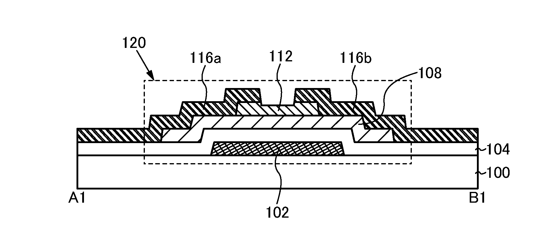
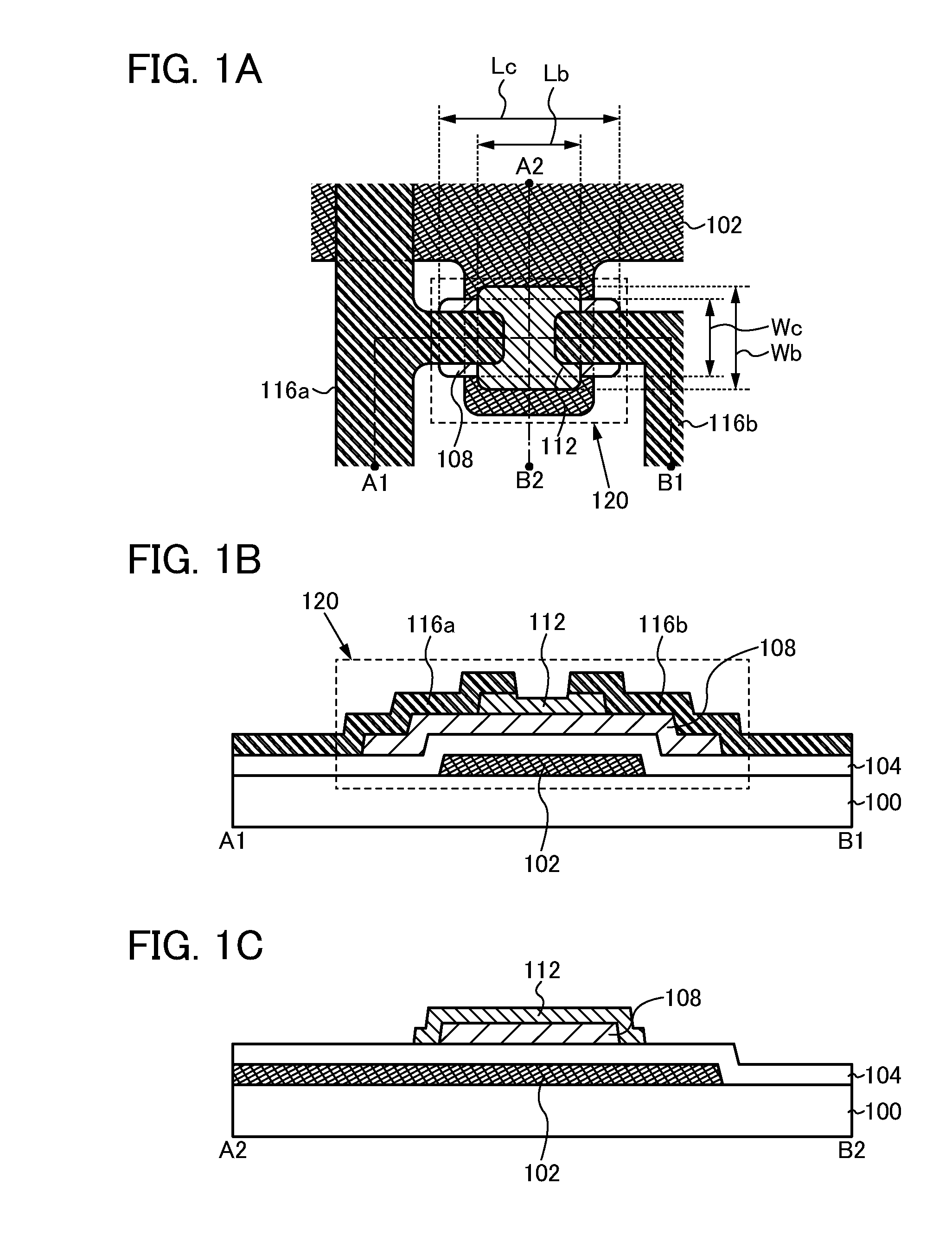
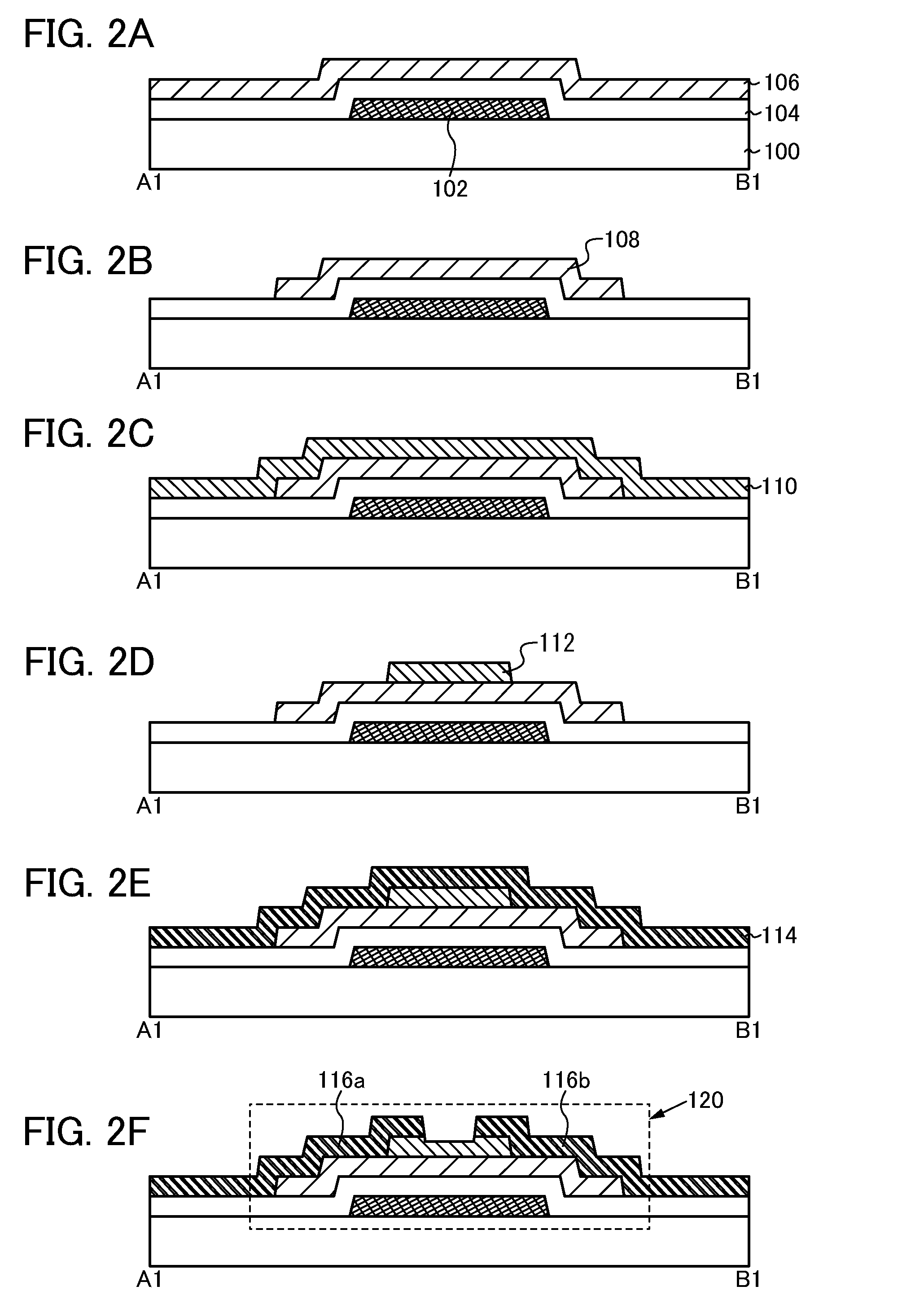
[0065]A transistor 120 illustrated in FIGS. 1A to 1C includes a gate (including a gate wiring and a gate electrode (hereinafter referred to as a “gate electrode 102”)) provided over a substrate 100, a gate insulating layer 104 provided over the gate electrode 102, an oxide semiconductor layer 108 provided over the gate insulating layer 104, a silicon layer 112 provided over and in contact with a surface of the oxide semiconductor layer 108, and a source (including a source wiring and a source electrode (hereinafter referred to as a “source electrode layer 116a”)) and a drain (including a drain wiring and a drain electrode (also referred to as a “drain electrode layer 116b”)) which are electrically connected to the oxide semiconductor layer 108 (see FIGS. 1A to 1C).
[0066]FIG. 1A is a top view, FIG. 1B is a cross-sectional view taken a...
embodiment 2
[0136]In this embodiment, a structure and a manufacturing method of a transistor which is different from that of Embodiment 1 will be described with reference to the drawings.
[0137]First, the manufacturing method of the transistor will be described with reference to FIGS. 5A to 5E. Note that the manufacturing process (such as applicable materials) described in this embodiment is in common with that of Embodiment 1 in many points. Thus, description of the common points is omitted below and only points different from those of Embodiment 1 will be described in detail.
[0138]First, a gate electrode 102 is formed over a substrate 100, and then a gate insulating layer 104 is formed over the gate electrode 102. Then, an oxide semiconductor layer 106 and a silicon layer 110 are sequentially formed to be stacked over the gate insulating layer 104, and a resist mask 171 is selectively formed (see FIG. 5A). It is preferable that layers of from the gate insulating layer 104 to the silicon layer ...
embodiment 3
[0150]In this embodiment, a transistor which is different from the transistors in Embodiments 1 and 2 and a manufacturing method thereof will be described with reference to the drawings. Note that the manufacturing process (such as applicable materials) described in this embodiment is in common with that of Embodiment 1 in many points. Thus, description of the common points is omitted below and only points different from those of Embodiment 1 will be described in detail.
[0151]A transistor 140 illustrated in FIGS. 7A and 7B includes a gate electrode 102 provided over a substrate 100, a gate insulating layer 104 provided over the gate electrode 102, an oxide semiconductor layer 108 provided over the gate insulating layer 104, a silicon layer 112 provided over and in contact with a surface of the oxide semiconductor layer 108, and a source electrode layer 116a and a drain electrode layer 116b provided over and in contact with the surface of the oxide semiconductor layer 108. In additio...
PUM
 Abstract
Description
Claims
Application Information


