Apparatus and method for manufacturing display panel, and display panel manufactured by the method

a technology of display panels and methods, which is applied in the manufacture of electrode systems, electric discharge tubes/lamps, instruments, etc., can solve the problems of increasing the footprint and the room for improvement in terms of achieve the effect of reducing manufacturing cost and apparatus cos

Inactive Publication Date: 2010-08-19
SHARP KK
View PDF6 Cites 50 Cited by
  • Summary
  • Abstract
  • Description
  • Claims
  • Application Information

AI Technical Summary

Benefits of technology

[0009]In view of the above problems, preferred embodiments of the present invention reduce the manufacturing cost and the apparatus cost for manufacturing a curved display panel as much as possible.

Problems solved by technology

S62-238526 requires multiple sets of rigid pressing jigs such as the male curved jig and the female curved jig, and also requires a space for installing or storing these multiple jigs, thereby increasing a footprint.
Thus, this manufacturing method still has room for improvement in terms of the manufacturing cost and the apparatus cost.

Method used


Image

  • Apparatus and method for manufacturing display panel, and display panel manufactured by the method
  • Apparatus and method for manufacturing display panel, and display panel manufactured by the method
  • Apparatus and method for manufacturing display panel, and display panel manufactured by the method

Examples


first preferred embodiment

[0071]FIGS. 1 through 8 show a first preferred embodiment of the present invention. Note that, in the preferred embodiments described below, a liquid crystal display (LCD) panel having a liquid crystal material enclosed between a pair of film substrates is described as an example of a display panel.

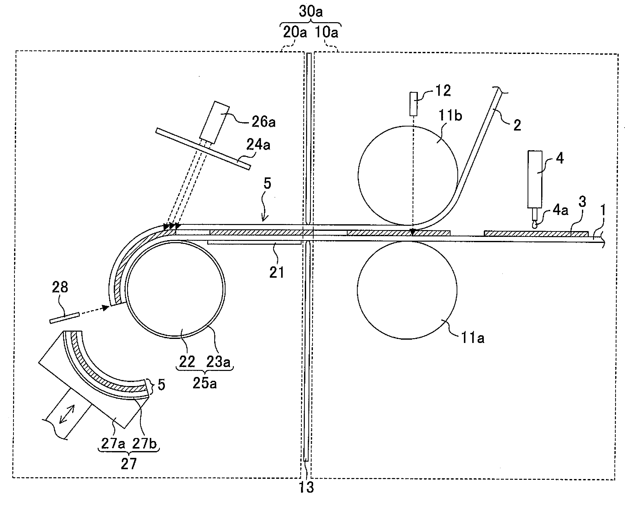
[0072]FIG. 1 is a side view of an LCD panel manufacturing apparatus 30a of the present preferred embodiment.

[0073]As shown in FIG. 1, the LCD panel manufacturing apparatus 30a includes a first processing unit 10a and a second processing unit 20a which are connected to each other through a pair of open / close gates 13. The LCD panel manufacturing apparatus 30a is configured to first form a bonded body 5 in the first processing unit 10a by successively bonding a TFT (Thin Film Transistor) film substrate 1 and a CF (Color Filter) film substrate 2, each having a plurality of display regions D (see FIG. 5) defined in a matrix pattern along the longitudinal direction and the width direction, thr...

second preferred embodiment

[0110]FIGS. 9 and 10 show a second preferred embodiment of the present invention. Note that, in the following preferred embodiments, the same elements as those of FIGS. 1 through 8 are denoted with the same reference numerals and characters as those of FIGS. 1 through 8, and detailed description thereof will be omitted.

[0111]The plastic film of the TFT film substrate 1 is an unprocessed film in the first preferred embodiment. In the present preferred embodiment, a half-cut groove H is formed along the width direction in every molding unit in the bottom surface of a plastic film of a TFT film substrate 1a.

[0112]A method for manufacturing an LCD panel using the TFT film substrate 1a will be described below with reference to FIGS. 9 and 10 mainly with respect to the differences from the manufacturing method described in the first preferred embodiment. FIG. 9 is a top view illustrating a dividing step of dividing a bonded body 5a of the present preferred embodiment, and FIG. 10 is a cr...

third preferred embodiment

[0124]FIGS. 11 and 12 show a third preferred embodiment of the present invention. FIG. 11 is a top view illustrating a dividing step of dividing a bonded body 5b of the present preferred embodiment, and FIG. 12 is a cross-sectional view of a region around the dividing cutter 28 taken along line XII-XII in FIG. 11.

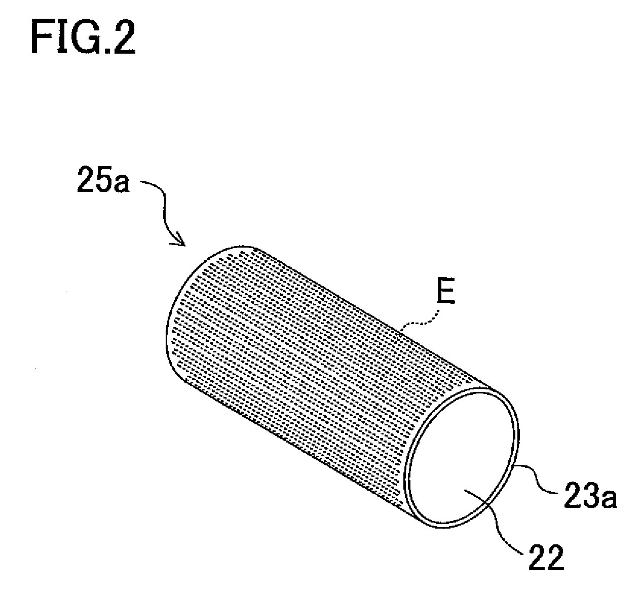
[0125]In the second preferred embodiment, the half-cut grooves H are formed in the bottom surface of the TFT film substrate 1a of the bonded body 5a in order to prevent any damage to the peripheral wall of the molding roll 25a. In the present preferred embodiment, as shown in FIG. 11, cut-outs C extending along the width direction are formed in a TFT film substrate 1b and a CF film substrate 2b of a bonded body 5b, and electrode patterns E in an electrostatic chuck layer 23b provided in a peripheral wall of a molding roll 25b have slit regions S formed at positions corresponding to the cut-outs C of the bonded body 5b. More specifically, in the bonded body 5b of the present...


PUM

PropertyMeasurementUnit
sizeaaaaaaaaaa
radiusaaaaaaaaaa
thickaaaaaaaaaa

Abstract

A liquid crystal display panel manufacturing apparatus for successively bonding a pair of film substrates, each having a plurality of display regions defined at least along a longitudinal direction, along the longitudinal direction through a sealant formed in every display region of one of the film substrates includes: a first processing unit arranged to form a bonded body by bonding the film substrates so that the respective display regions are superimposed on each other; and a second processing unit including a molding roll configured to hold the bonded body formed in the first processing unit onto a peripheral wall thereof, and arranged to mold the bonded body into a curved shape along the peripheral wall of the molding roll by curing the sealant while holding the bonded body on the peripheral wall of the molding roll.

Description

BACKGROUND OF THE INVENTION[0001]1. Field of the Invention[0002]The present invention generally relates to an apparatus and a method for manufacturing a display panel, and a display panel manufactured by the method. More particularly, the present invention relates to a manufacturing technique of a curved display panel.[0003]2. Description of the Related Art[0004]Flexible display panels using flexible film substrates instead of conventionally used glass substrates have been developed in the fields of liquid crystal displays, organic EL (Electro Luminescence) displays, and the like.[0005]For example, Japanese Published Patent Application No. S62-150219 discloses a manufacturing method of a flexible electrooptic device in which evacuation and injection are performed on every predetermined number of cells without cutting a band-shaped cell substrate. Japanese Published Patent Application No. S62-150219 describes that this method significantly reduces the injection time of a liquid mater...

Claims


Application Information

Patent Timeline
Patent Type & Authority Applications(United States)
IPC IPC(8): G02F1/1339B32B37/10H01J9/46G02F1/1333
CPCG02F1/1303G02F1/133305Y10T156/1043G02F2001/133354G02F1/1341G02F1/133354
Inventor YOSHIDA, TOKUO
Owner SHARP KK
Why Eureka
Try Eureka