Method to assemble nano-structure on a substrate and nano-molecule device comprising nano-structure formed thereby

a nano-structure and substrate technology, applied in the direction of nanostructure assembly, instruments, photomechanical equipment, etc., can solve the problems of nano-structure contamination, difficult to control the nanostructure, and difficult to adjust the direction of the nanoline in a local area

Active Publication Date: 2010-08-26
RES & BUSINESS FOUND SUNGKYUNKWAN UNIV
View PDF1 Cites 11 Cited by
  • Summary
  • Abstract
  • Description
  • Claims
  • Application Information

AI Technical Summary

Benefits of technology

[0009]An advantage of some aspects of the invention is that it provides a method of sele

Problems solved by technology

However, since the sizes of the nanostructures are very small, it is very difficult to control the nanostructures.
In this case, many nanolines can be arranged in the same direction in a large area, but it is very difficult to adjust the direction of the nanolines in a local area.
However, this method has a problem that th

Method used


Image

  • Method to assemble nano-structure on a substrate and nano-molecule device comprising nano-structure formed thereby
  • Method to assemble nano-structure on a substrate and nano-molecule device comprising nano-structure formed thereby
  • Method to assemble nano-structure on a substrate and nano-molecule device comprising nano-structure formed thereby

Examples


Embodiment Construction

[0030]Hereinafter, exemplary embodiments of the invention will be described in detail with reference to the accompanying drawings.

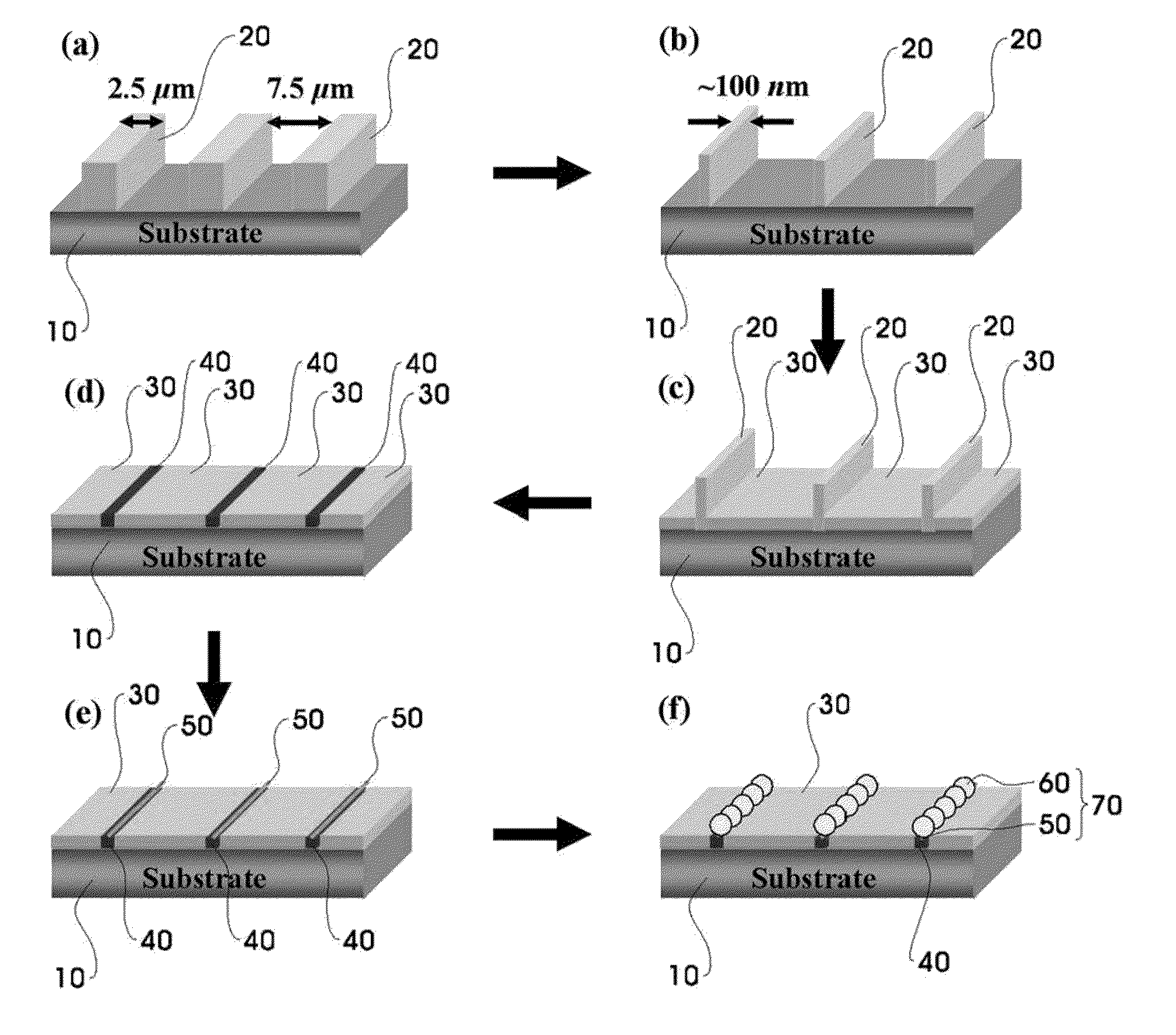
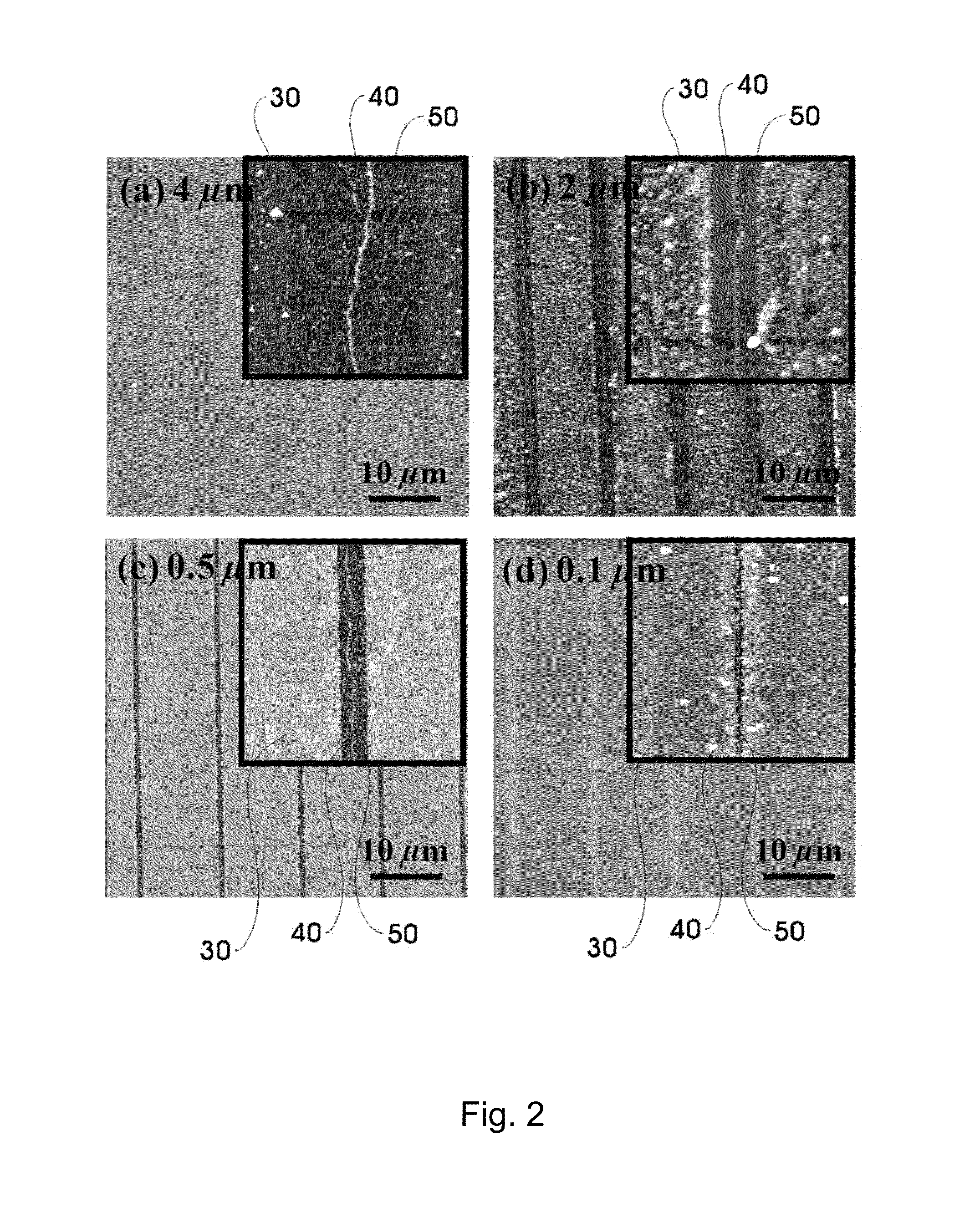
[0031]FIGS. 1A to 1F are diagrams schematically illustrating a procedure of selectively positioning nanostructures on a substrate according to an embodiment of the invention.

[0032]FIG. 1A shows a state where a photoresist pattern having a line width in the micrometer unit is formed on a substrate.

[0033]The substrate 10 may employ an Si wafer, a wafer having SiO2 deposited thereon, a glass substrate, a glass substrate coated with a transparent conductive oxide film, a flexible substrate such as polyimide. A photoresist pattern 20 having a line width in the micrometer unit is formed on the substrate 10 using a photolithography process. Here, the photoresist pattern may be formed in an intersecting or lattice shape, not a single straight line.

[0034]FIG. 1B shows a state where a photoresist pattern having a line width in the nanometer unit is formed on the su...


PUM


Abstract

A method of selectively positioning nanostructures on a substrate is provided which includes: a first step of forming a photoresist pattern on the substrate and then control the line width of the photoresist pattern in a nano unit to form a nanometer photoresist layer; a second step of forming a protective layer for preventing adsorption of a nano-material in a patter-unformed area on the substrate on which the nanometer photoresist layer has been formed; a third step of removing the photoresist layer formed on the substrate; a fourth step of forming a positively-charged or negatively charged adsorbent layer in the area from which the photoresist layer has been removed; and a fifth step of applying a nano-material-containing solution charged in the opposite polarity of the adsorbent layer to the substrate on which the adsorbent layer has been formed.

Description

CROSS REFERENCE TO PRIOR APPLICATIONS[0001]This application claims priority of Korean Patent Application No. 10-2009-0013339 filed 18 Feb. 2009, which is hereby incorporated herein by reference in its entirety.BACKGROUND[0002]1. Field of the Invention[0003]The present invention relates to a method of manufacturing a selective nanoline, and more particularly, to a method of selectively arranging and positioning nanostructures on a substrate.[0004]2. Description of the Related Art[0005]With the recent advancement in semiconductor technology, electronic elements have decreased in size to a nanometer size and have increased in a degree of integration. Particularly, elements such as CMOS have been widely used in the field of large-scaled integrated circuits and line widths of the elements have decreased with the increase in a degree of integration. Nano-elements have been drastically studied with the decrease in size of the elements. A process of arranging nanometer lines at specific pos...

Claims


Application Information

Patent Timeline
IPC IPC(8): G03F7/20
CPCB81C1/00031B82B3/0052B82Y40/00B82Y30/00B82B1/00B82B3/00
Inventor HONG, BYUNG YOUKIM, HYUNG JINROH, YOUNG HAN
Owner RES & BUSINESS FOUND SUNGKYUNKWAN UNIV
Why Eureka
Try Eureka