Eureka AIR delivers breakthrough ideas for toughest innovation challenges, trusted by R&D personnel around the world.

Transfer of high temperature wafers

Inactive Publication Date: 2010-08-26
S O I TEC SILICON ON INSULATOR THECHNOLOGIES
View PDF9 Cites 1 Cited by
  • Summary
  • Abstract
  • Description
  • Claims
  • Application Information

AI Technical Summary

Benefits of technology

[0005]The present invention comprises methods and apparatus to limit or prevent surface decomposition or sublimation, congruent or otherwise (collectively, referred to herein as “surface changes” or “surface damage”) of planar, compound semiconductor materials (also known herein as “wafers”) during their loading and unloading from a process reactor such as a growth chamber at process temperatures (which can be up to 1,000° C. and above). Decomposition or sublimation of a wafer surface can degrade or damage wafer quality, and limiting or preventing such changes is clearly desirable. Loading and unloading at process temperatures are desirable in order to minimize the times for temperature ramp-up and ramp-down during semiconductor processing. These processes thereby can have increased throughput, and process equipment systems can have higher effective utilizations.
[0010]However, to limit or prevent surface changes during high temperature transfer, this invention uses gas streams comprising active gas components to generate the wafer-controlling aerodynamic forces. The concentration of the active gas components is chosen in view of the composition of the wafer surface and of the expected transfer temperatures. The gas streams can also comprise selected inert or inactive components depending on the designated growth in the reactor and may include the addition of carrier species to improve process flexibility. Consequently, active gas ejection from the Bernoulli wand fixture of the invention enables wafer loading and unloading without surface deterioration while above temperatures at which surface deterioration (decomposition temperatures or congruent or non-congruent sublimation temperatures) of the specific compound semiconductor is likely.
[0012]Thus, when such a semiconductor wafer is transferred by a transfer device of this invention discharging such active gases, the wafer surface is protected from degradation even if at high temperatures. Further, aerodynamic forces generated by the discharged gases can act to suspend a wafer beneath the transfer device (particularly, beneath the head of the transfer device). Accordingly, in various embodiments, this invention can also include a wafer transfer device with a semiconductor wafer suspended beneath the device and bathed by active gases that act to protect the wafer from degradation even at high temperatures.
[0015]The invention also provides various embodiments of semiconductor wafer transfer methods that can be advantageously applied to transferring semiconductor wafers between a growth environment, e.g., a CVD reactor chamber, where the wafer resides during periods of epitaxial growth, and a transfer environment, where the wafer resides before, between, or after periods of epitaxial growth. According to the provided methods, during wafer transfer between these two environments, at least one surface of the wafer is bathed with gases having an active portion that is chemically reactive with the wafer surface in a manner so as to limit its decomposition or sublimation. Optionally, the wafer can continue to be bathed in the transfer-to environment for a period of time until there is little risk of surface decomposition or sublimation in the new environment, or the wafer can be bathed for a time in the transfer-from environment in order to prepare for transfer. Preferably, the wafer is suspended during transfer by aerodynamic forces generated by the gases bathing the wafer surface.

Problems solved by technology

Above known critical temperatures, surfaces of compound semiconductors can be impaired or damaged by, for example, evaporation of one or more of the more volatile species from the surface.
However, heretofore, such wands have been first and foremost used for the transfer of silicon wafers, which are incapable of undergoing a congruent sublimation type of decomposition and are therefore subject to less rigorous reactor transfer protocols.
Conversely, compound semiconductor wafers, which are subject to such damage, commonly require highly controlled heating and cooling procedures to ensure the wafer temperature is below the congruent sublimation temperature prior to loading / unloading of the wafer to or from the process reactor.
Although the cooling process is invaluable for preserving the high quality surface of the compound semiconductor, the time taken represents a significant loss in production with the subsequent financial consequences.

Method used


Image

  • Transfer of high temperature wafers
  • Transfer of high temperature wafers
  • Transfer of high temperature wafers

Examples


Embodiment Construction

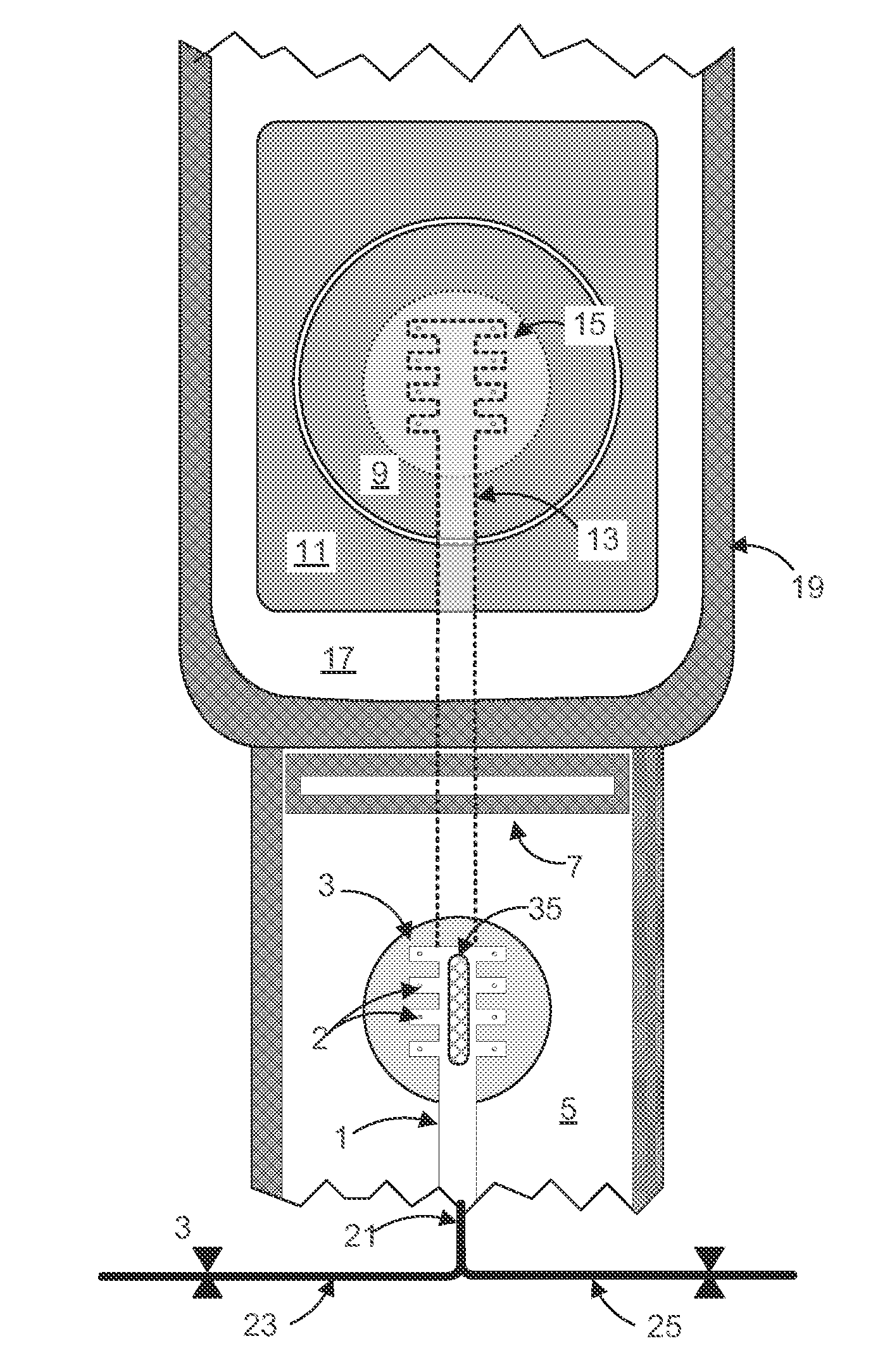
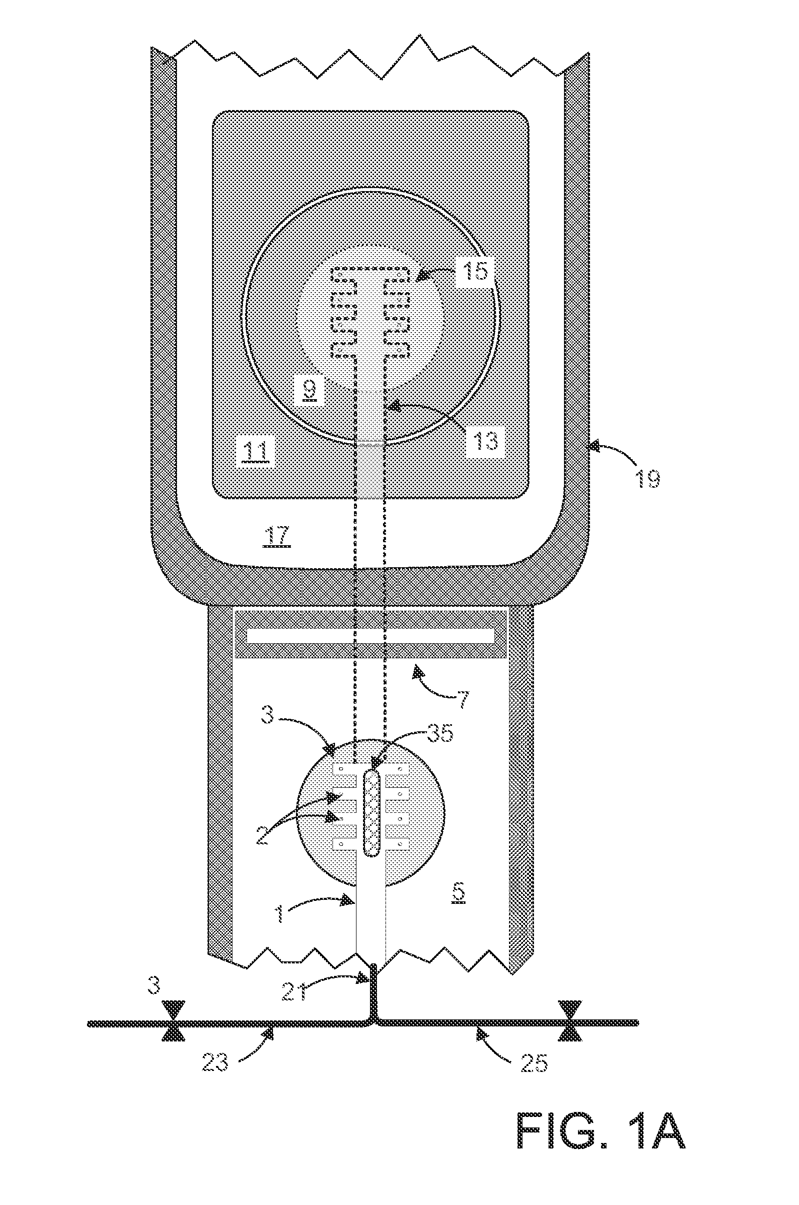
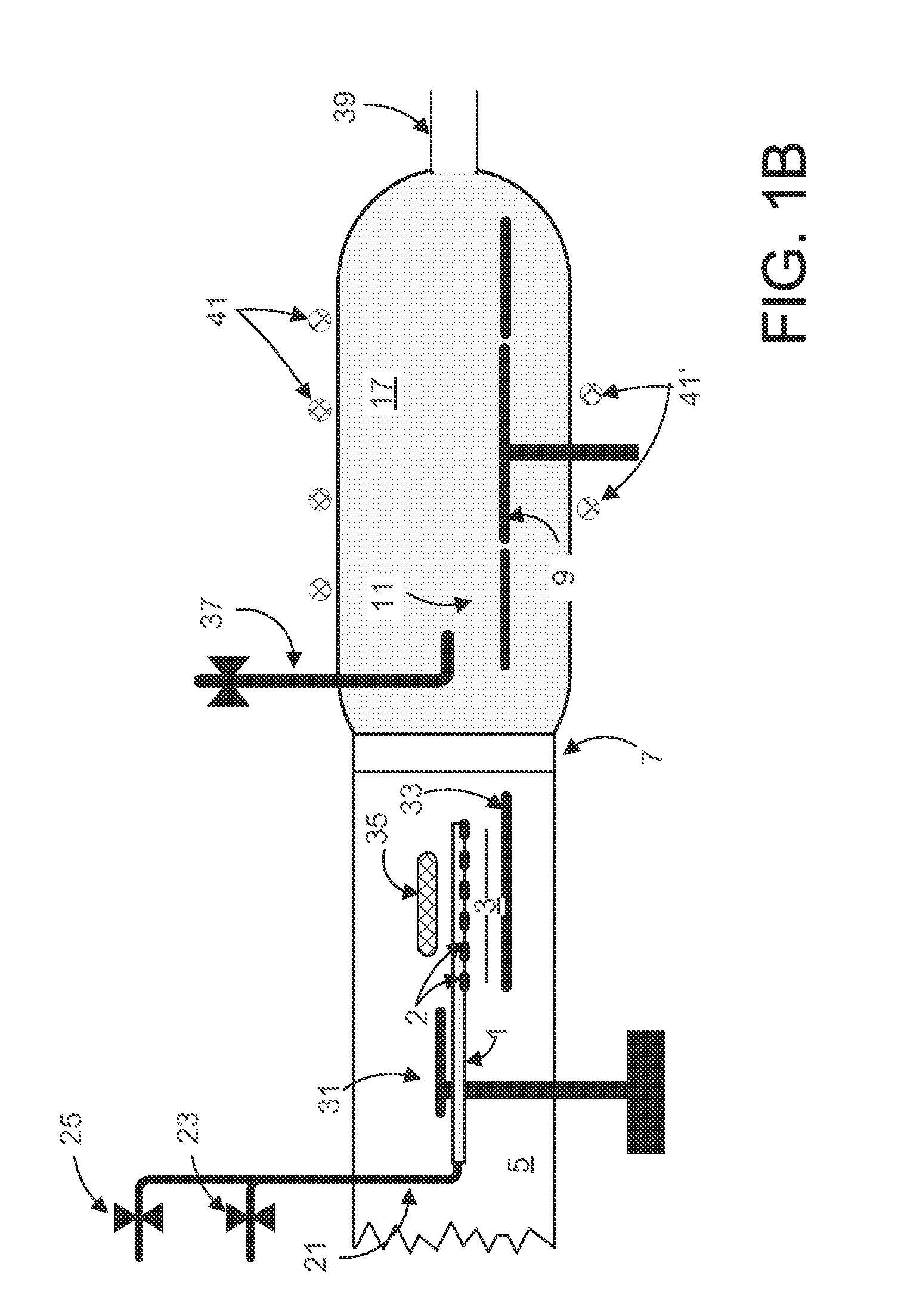
[0025]Preferred embodiments of the invention are now described. It should be understood that the preferred embodiment using Bernoulli wands are not limiting and other embodiments of this invention do not use Bernoulli wands. Headings are used herein for clarity only and without any intended limitation.

[0026]The words “significant” and “likely” (and similar words of degree) are used here to mean within acceptable and expected limits, usually commercially-acceptable limits. For example, in the phrase “significant wafer damage is unlikely in the process”, the phrase “significant wafer damage” is taken to mean damage that limits or prevents intended, usually commercial, applications of the wafer. The phrase “unlikely in the process” is taken to mean that, although significant damage may occur, it occurs sufficiently rarely that commercial use of the process is not hindered or prevented. The ranges signified by these terms depend on commercial requirements (or research requirements, or t...


PUM

PropertyMeasurementUnit
Temperatureaaaaaaaaaa
Forceaaaaaaaaaa

Abstract

This invention provides apparatus, protocols, and methods that permit wafers to be loaded and unloaded in a gas-phase epitaxial growth chamber at high temperatures. Specifically, this invention provides a device for moving wafers or substrates that can bath a substrate being moved in active gases that are optionally temperature controlled. The active gases can act to limit or prevent sublimation or decomposition of the wafer surface, and can be temperature controlled to limit or prevent thermal damage. Thereby, previously-necessary temperature ramping of growth chambers can be reduced or eliminated leading to improvement in wafer throughput and system efficiency.

Description

FIELD OF THE INVENTION[0001]The present invention is related to the field of semiconductor processing equipment, and specifically provides apparatus and methods that permit a gas-phase epitaxial growth chamber to be loaded and unloaded at high temperatures heretofore unachievable. Specifically, this invention provides a device for moving wafers or substrates that can bathe a substrate being moved in active gases that are optionally temperature controlled.BACKGROUND OF THE INVENTION[0002]Above known critical temperatures, surfaces of compound semiconductors can be impaired or damaged by, for example, evaporation of one or more of the more volatile species from the surface. One form of this evaporation point is known as “sublimation”, in particular “congruent sublimation”. For example, in the case of gallium nitride, the onset of surface decomposition, primarily by loss of nitrogen, begins above a temperature of the order of 800° C., see Mastro et al., 2005, J. of Crystal Growth 274:3...

Claims


Application Information

Patent Timeline
IPC IPC(8): H01L21/30
CPCH01L21/6838H01L21/67748
Inventor TISCHLER, MICHAEL ALBERTBERTRAM, JR., RONALD THOMAS
Owner S O I TEC SILICON ON INSULATOR THECHNOLOGIES
Why Eureka
Eureka Blog
Learn More