CMOS Transistors With Silicon Germanium Channel and Dual Embedded Stressors

a technology of stressors and transistors, applied in the field of semiconductor devices, can solve the problems of becoming more and more difficult to apply strong stress in both nfet and pfet channels with stress liners, and achieve the effect of enhancing electron mobility and hole mobility

Active Publication Date: 2010-09-09
GLOBALFOUNDRIES US INC
View PDF2 Cites 101 Cited by
  • Summary
  • Abstract
  • Description
  • Claims
  • Application Information

AI Technical Summary

Benefits of technology

[0009]The present invention provides a semiconductor structure including a p-type MOSFET and an n-type MOSFET. The p-type MOSFET has a silicon-germanium alloy channel to which a longitudinal compressive stress is applied by embedded epitaxial silicon-germanium alloy source and drain regions comprising a silicon-germanium alloy having a higher concentration of germanium than the channel of the p-type MOSFET. The n-type MOSFET has a silicon-germanium alloy channel to which a longitudinal tensile stress is applied by embedded epitaxial silicon source and drain regions comprising silicon. The silicon-germanium alloy channel in the p-type MOSFET provides enhanced hole mobility, while the silicon-germanium alloy channel in the n-type MOSFET provides enhanced electron mobility, thereby providing performance improvement to both the p-type MOSFET and the n-type MOSFET.

Problems solved by technology

While such beneficial effects of stress are known in the art, a difficulty arises since two different types of field effect transistors require two different types of stress.
With scaling down of the critical dimension, it becomes more and more difficult to apply strong stress in both NFET and PFET channel with stress liners.

Method used


Image

  • CMOS Transistors With Silicon Germanium Channel and Dual Embedded Stressors
  • CMOS Transistors With Silicon Germanium Channel and Dual Embedded Stressors
  • CMOS Transistors With Silicon Germanium Channel and Dual Embedded Stressors

Examples


Embodiment Construction

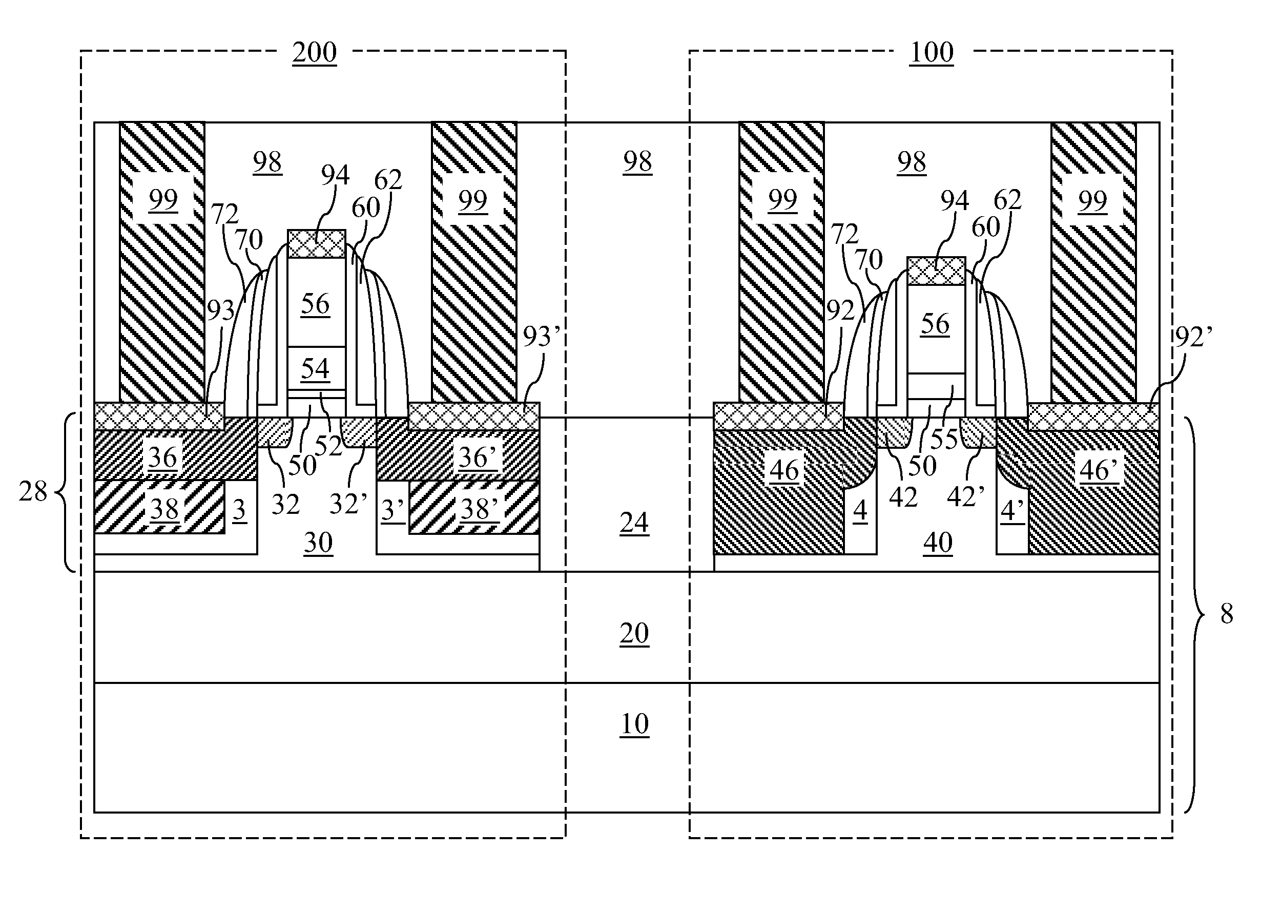
[0030]As stated above, the present invention relates to complementary metal-oxide-semiconductor (CMOS) field effect transistors having a silicon-germanium alloy channel and dual stressors for generating tensile or compressive longitudinal stress along the channel, and methods of manufacturing the same, which are now described in detail with accompanying figures. The drawings are not necessarily drawn to scale.

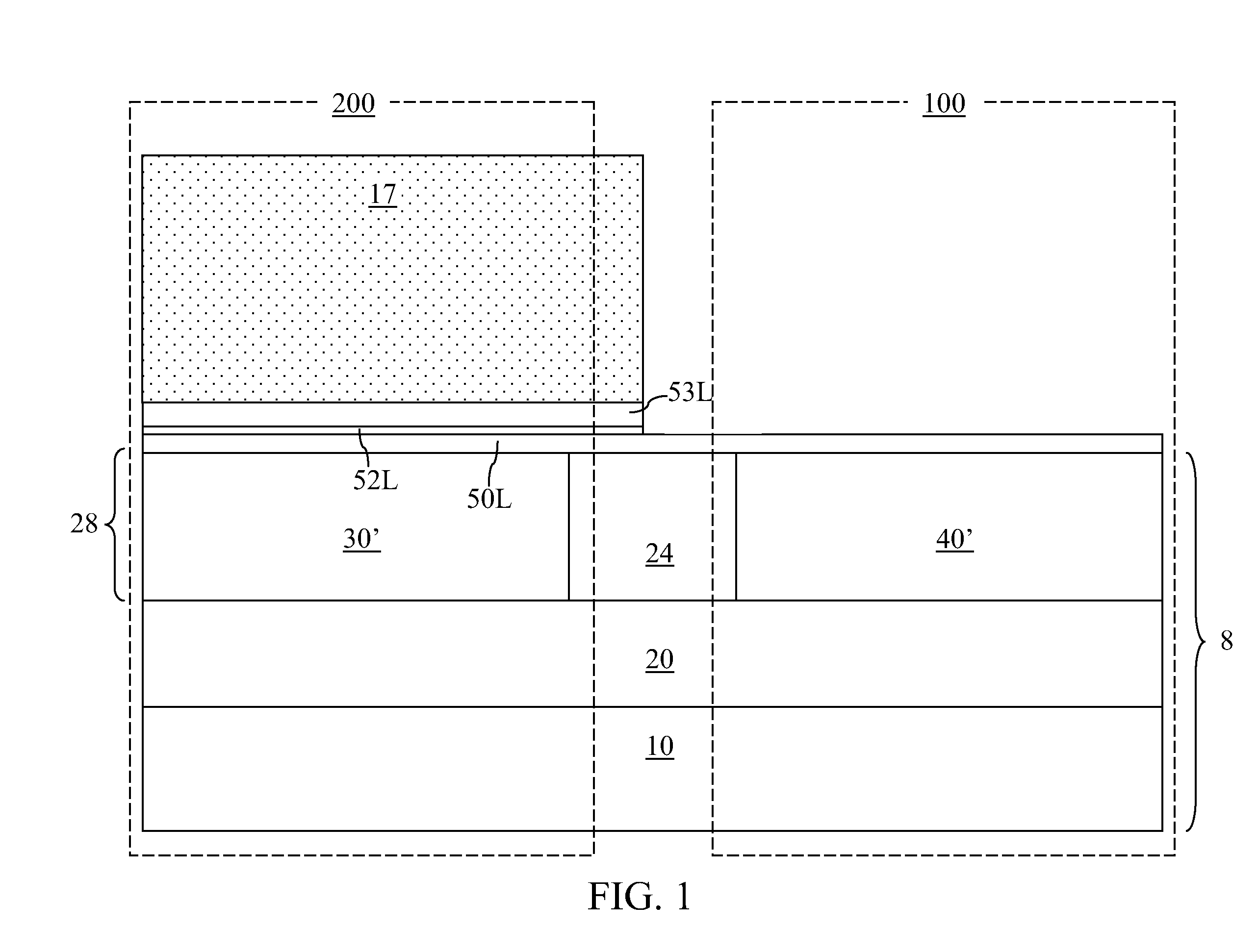
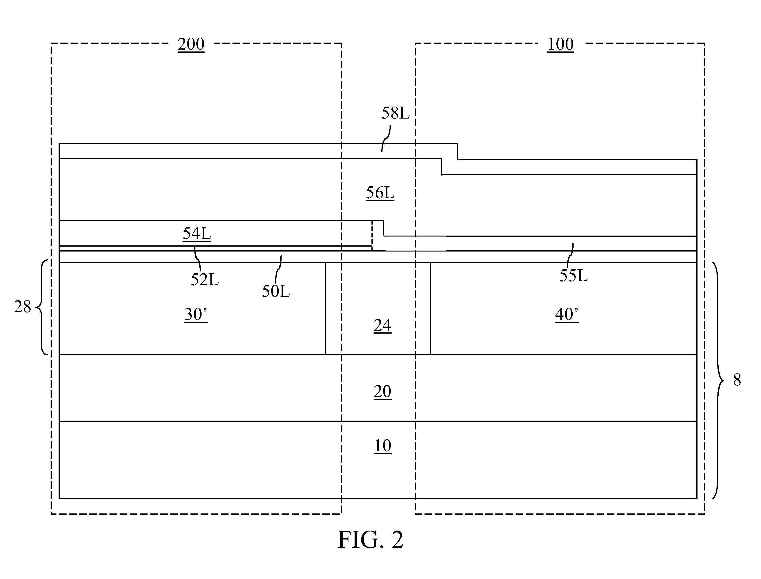
[0031]Referring to FIG. 1, an exemplary semiconductor structure according to the present invention is shown, which includes a semiconductor substrate 8 including a bottom substrate layer 10, an intermediate substrate layer 20, and a top semiconductor layer 28. The top semiconductor layer 28 includes a first top semiconductor portion 40′ located in a first device region 100 and a second top semiconductor layer 30′ located in a second device region 200. The top semiconductor layer 28 includes a shallow trench isolation structure 24, which straddles the first device region 100 and...


PUM

PropertyMeasurementUnit
thicknessesaaaaaaaaaa

Abstract

A p-type MOSFET of a CMOS structure has a silicon-germanium alloy channel to which a longitudinal compressive stress is applied by embedded epitaxial silicon-germanium alloy source and drain regions comprising a silicon-germanium alloy having a higher concentration of germanium than the channel of the p-type MOSFET. An n-type MOSFET of the CMOS structure has a silicon-germanium alloy channel to which a longitudinal tensile stress is applied by embedded epitaxial silicon source and drain regions comprising silicon. The silicon-germanium alloy channel in the p-type MOSFET provides enhanced hole mobility, while the silicon-germanium alloy channel in the n-type MOSFET provides enhanced electron mobility, thereby providing performance improvement to both the p-type MOSFET and the n-type MOSFET.

Description

[0001]This non-provisional application claims the benefit of the provisional application filed with the United States Patent and Trademark Office as Ser. No. 61 / 156,960 entitled “CMOS Transistors With Silicon Germanium Channel and Dual Embedded Stressors”, filed Mar. 3, 2009.FIELD OF THE INVENTION [0002]The present invention generally relates to semiconductor devices, and particularly to complementary metal-oxide-semiconductor (CMOS) field effect transistors having a silicon-germanium alloy channel and dual stressors for generating tensile or compressive longitudinal stress along the channel, and methods of manufacturing the same.BACKGROUND OF THE INVENTION[0003]Carrier mobility in a metal oxide semiconductor field effect transistor (MOSFET) may be manipulated by a stress applied to the channel of the MOSFET. Even relatively small changes in the stress of the channel may result in large changes in carrier mobility for some combinations of semiconductor material and crystallographic ...

Claims


Application Information

Patent Timeline
Patent Type & Authority Applications(United States)
IPC IPC(8): H01L27/092H01L29/78H01L21/336
CPCH01L21/823807H01L21/823814H01L27/092H01L29/1054H01L29/165H01L29/7848H01L29/6656H01L29/6659H01L29/66636H01L29/66651H01L29/7833H01L29/665
Inventor ZHU, HUILONG
Owner GLOBALFOUNDRIES US INC
Why Eureka
Try Eureka