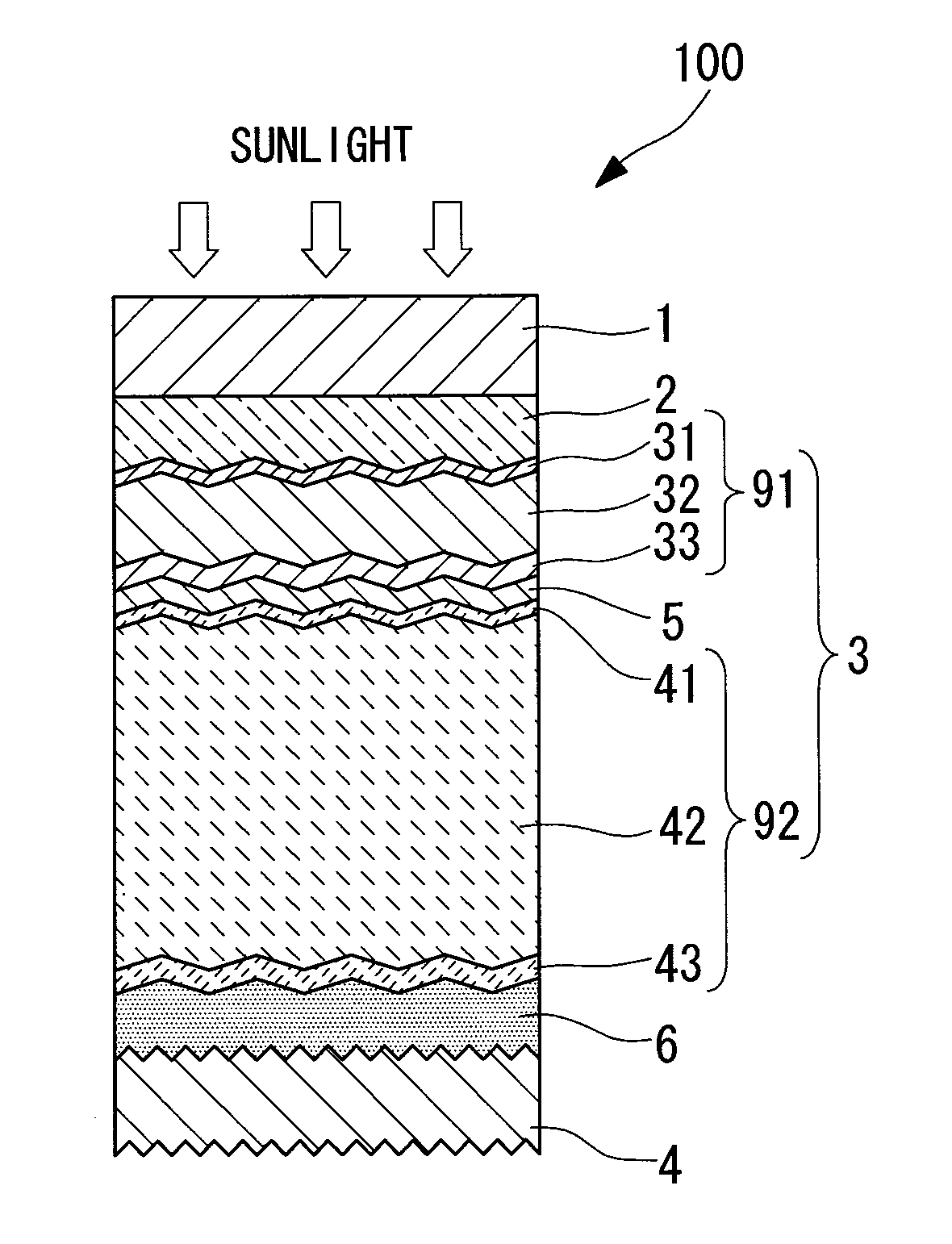
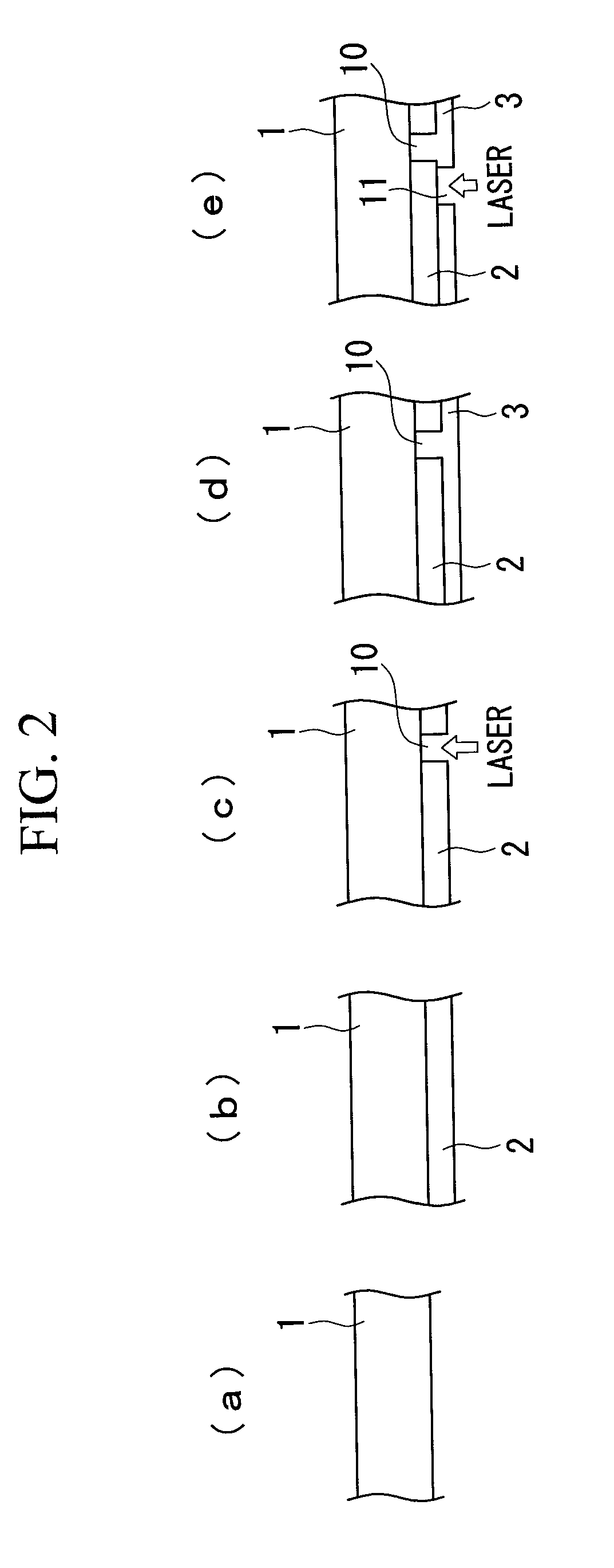
Photovoltaic device

a photovoltaic and solar cell technology, applied in the field of photovoltaic devices, can solve the problems of increasing the short-circuit the internal transparency of the transparent conductive layer, and the short-circuit current of the solar cell, and achieves the effects of increasing the quantity of light absorbed, increasing the short-circuit current, and high-efficiency production

Inactive Publication Date: 2010-09-16
MITSUBISHI HEAVY IND LTD
View PDF0 Cites 5 Cited by
  • Summary
  • Abstract
  • Description
  • Claims
  • Application Information

AI Technical Summary

Benefits of technology

[0020]The thin films listed above all exhibit high reflectance, and therefore increase the quantity of light absorbed by the electric power generation layer, enabling an increase in the short-circuit current at the electric power generation layer.
[0021]In a photovoltaic device according to one aspect of the present invention, the film thickness of the second transparent electrode layer is not less than 80 nm and not more than 100 nm, and the light absorptance for the second transparent electrode layer in a wavelength region from not less than 600 nm to not more than 1,000 nm is not more than 1.5%, and consequently the quantity of light absorption at the electric power generation layer increases, yielding a photovoltaic device having a high short-circuit current.
[0022]In a photovoltaic device according to another aspect of the present invention, the film thickness of the second transparent electrode layer is not less than 80 nm and not more than 100 nm, and the reflectance for light reflected at the interface between the second transparent electrode layer and the electric power generation layer, and at the interface between the second transparent electrode layer and the back electrode layer is not less than 91% in the wavelength region from not less than 600 nm to not more than 1,000 nm, and consequently the quantity of light absorption at the electric power generation layer increases, yielding a photovoltaic device having a high short-circuit current.

Problems solved by technology

The deposition conditions for the above transparent conductive layer have yet to be optimized, and problems remain with the internal transparency of the transparent conductive layer.
When a transparent conductive layer is formed, light absorption by the transparent conductive layer represents a loss that causes a decrease in the short-circuit current of the solar cell.
As a result, improving the transparency of the transparent conductive layer, thereby increasing the short-circuit current of the solar cell, has become an important issue.

Method used


Image

  • Photovoltaic device
  • Photovoltaic device
  • Photovoltaic device

Examples


examples

Optical Thin Film Calculations

[0092]Optical thin film interference calculations based on Fresnel reflections were conducted for models having a GZO film for which the light absorption (transparency) exhibited (A) a small light absorptance, (B) a medium light absorptance, or (C) a large light absorptance. OPTAS-FILM from Cybernet Systems Co., Ltd. was used as the calculation software. Data disclosed in existing literature was used as the medium data for the glass and the silver thin film. The medium data for the GZO film was determined by optical measurement of a GZO film formed on glass. Data for monocrystalline Si disclosed in existing literature was used as the medium data for the crystalline silicon. Air was assumed to have a refractive index of 1 and an extinction coefficient of 0.

[0093]Absorption spectra were calculated for a structural model (structural model 1) comprising a GZO film exhibiting the light absorption of (A), (B) or (C) formed on top of a glass substrate. The gla...


PUM


Abstract

The short-circuit current of a photovoltaic device is improved by optimizing the transparent conductive layer. A photovoltaic device comprising a first transparent electrode layer, an electric power generation layer, a second transparent electrode layer and a back electrode layer on a substrate, wherein the film thickness of the second transparent electrode layer is not less than 80 nm and not more than 100 nm, and the light absorptance for the second transparent electrode layer in a wavelength region from not less than 600 nm to not more than 1,000 nm is not more than 1.5%. Also, a photovoltaic device wherein the film thickness of the second transparent electrode layer is not less than 80 nm and not more than 100 nm, and the reflectance for light reflected at the second transparent electrode layer and the back electrode layer is not less than 91% in the wavelength region from not less than 600 nm to not more than 1,000 nm.

Description

TECHNICAL FIELD[0001]The present invention relates to a photovoltaic device, and relates particularly to a solar cell that uses silicon as the electric power generation layer.BACKGROUND ART[0002]The use of solar cells as photovoltaic devices that receive light and convert the energy into electrical power is already known. Amongst solar cells, thin-film type solar cells in which thin films of silicon-based layers are stacked together to form an electric power generation layer (photovoltaic layer) offer various advantages, including the comparative ease with which the surface area can be increased, and the fact that the film thickness is approximately 1 / 100th that of a crystalline solar cell, meaning minimal material is required. As a result, thin-film silicon-based solar cells can be produced at lower cost than crystalline solar cells. However, a drawback of thin-film silicon-based solar cells is the fact that the conversion efficiency is lower than that of crystalline solar cells.[0...

Claims


Application Information

Patent Timeline
Patent Type & Authority Applications(United States)
IPC IPC(8): H01L31/0224H01L31/04H01L31/028
CPCH01L21/02554H01L21/02573H01L21/02631H01L31/022466H01L31/0547H01L31/0687H01L31/1884Y02E10/52Y02E10/544H01L31/0236H01L31/022483H01L31/02366Y02E10/547
Inventor SAKAI, SATOSHIASAHARA, YUJIKOBAYASHI, YASUYUKIMORI, MASAFUMITSURUGA, SHIGENORIYAMASHITA, NOBUKI
Owner MITSUBISHI HEAVY IND LTD
Why Eureka
Try Eureka