

Light-emitting element, light-emitting device, display, and electronic equipment
a technology of light-emitting elements and light-emitting devices, which is applied in the direction of semiconductor devices, diodes, electrical equipment, etc., can solve the problems of reducing the lifetime of light-emitting elements and deteriorating light-emitting layers on the cathode side, and achieve high-reliability electronic equipment
- Summary
- Abstract
- Description
- Claims
- Application Information
AI Technical Summary
Benefits of technology
Problems solved by technology
Method used
Image

Examples
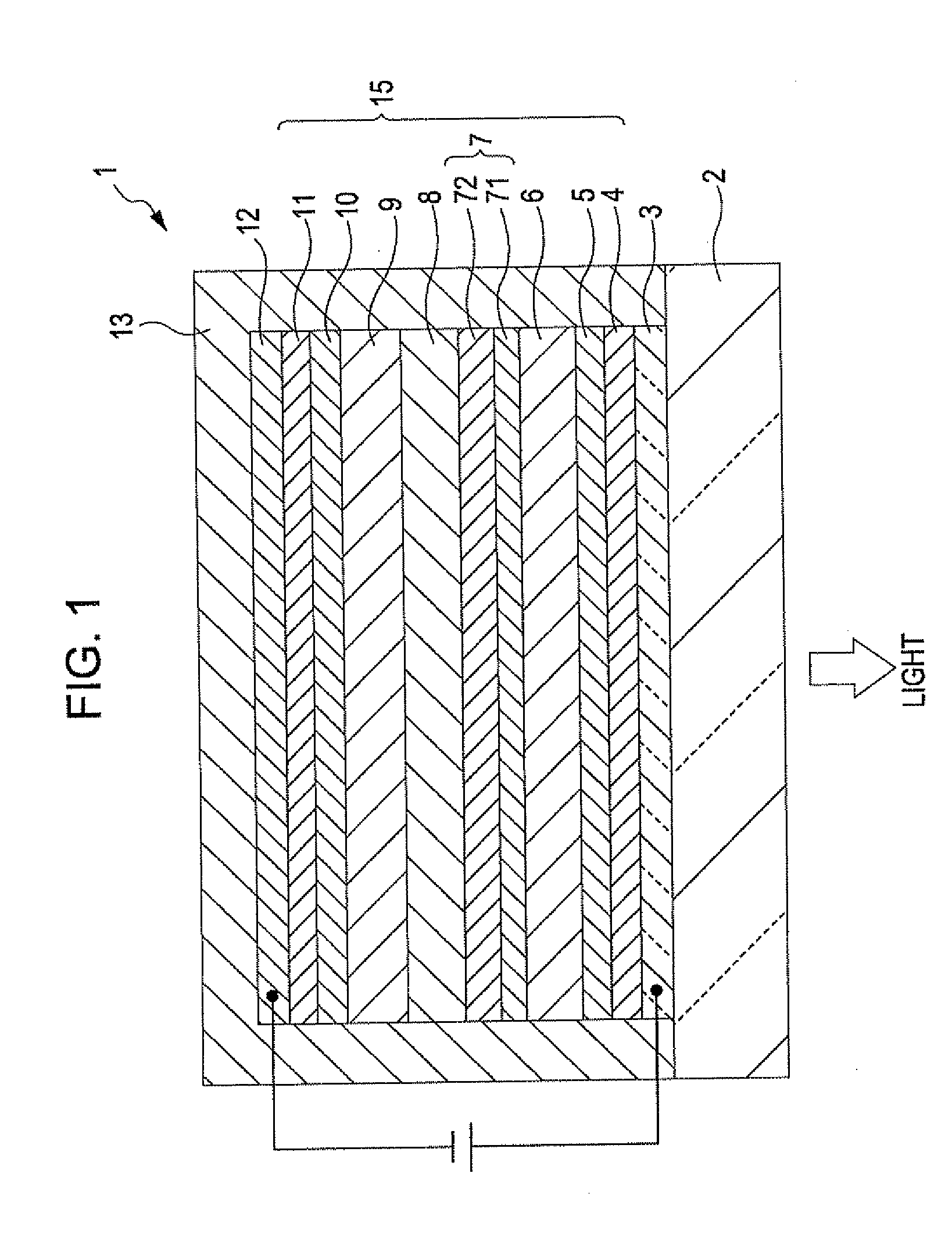
example 1
[0218](1) First, a transparent glass substrate having an average thickness of 0.5 mm was prepared. Then, an ITO electrode (anode) with an average thickness of 100 nm was formed on the substrate by sputtering.
[0219]Then, the substrate was immersed in acetone and then in 2-propanol for ultrasonic cleansing, followed by oxygen plasma treatment.
[0220](2) Then, m-MTDATA represented by the above-mentioned formula 1 was vapor-deposited on the ITO electrode by vacuum vapor deposition to form a hole injection layer with an average thickness of 30 nm.
[0221](3) Then, α-NPD represented by the above-mentioned formula 5 was vapor-deposited on the hole injection layer by vacuum vapor deposition to form a hole-transporting layer with an average thickness of 20 nm.
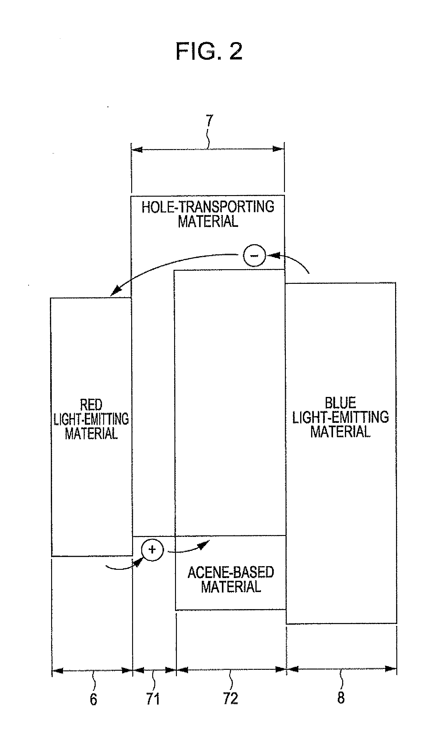
[0222](4) Then, constituent materials of a red light-emitting layer were vapor-deposited on the hole-transporting layer by vacuum vapor deposition to form a red light-emitting layer (first light-emitting layer) with an average thickness of...
example 2
[0233]A light-emitting element was produced as in Example 1, except that the thickness of the first layer of the intermediate layer was 3 nm.
example 3
[0234]A light-emitting element was produced as in Example 1, except that the thickness of the first layer of the intermediate layer was 1 nm.
PUM
 Abstract
Description
Claims
Application Information