Trench generated device structures and design structures for radiofrequency and bicmos integrated circuits

a technology of integrated circuits and device structures, applied in semiconductor devices, instruments, computing, etc., can solve the problems of bipolar junction transistors having a conventional vertically stacked arrangement, difficult fabrication of bipolar junction transistors in such thin layers of silicon, and the ideality of such diodes is generally greater than unity, and the diodes are less than ideal for many analog applications

Active Publication Date: 2010-09-16
GLOBALFOUNDRIES US INC
View PDF35 Cites 16 Cited by
  • Summary
  • Abstract
  • Description
  • Claims
  • Application Information

AI Technical Summary

Problems solved by technology

Fabrication of bipolar junction transistors having a conventional vertically stacked arrangement can be difficult in such thin layers of silicon.
Although lateral p-n junctions can be built in thin SOI layers, the ideality of

Method used


Image

  • Trench generated device structures and design structures for radiofrequency and bicmos integrated circuits
  • Trench generated device structures and design structures for radiofrequency and bicmos integrated circuits
  • Trench generated device structures and design structures for radiofrequency and bicmos integrated circuits

Examples


Embodiment Construction

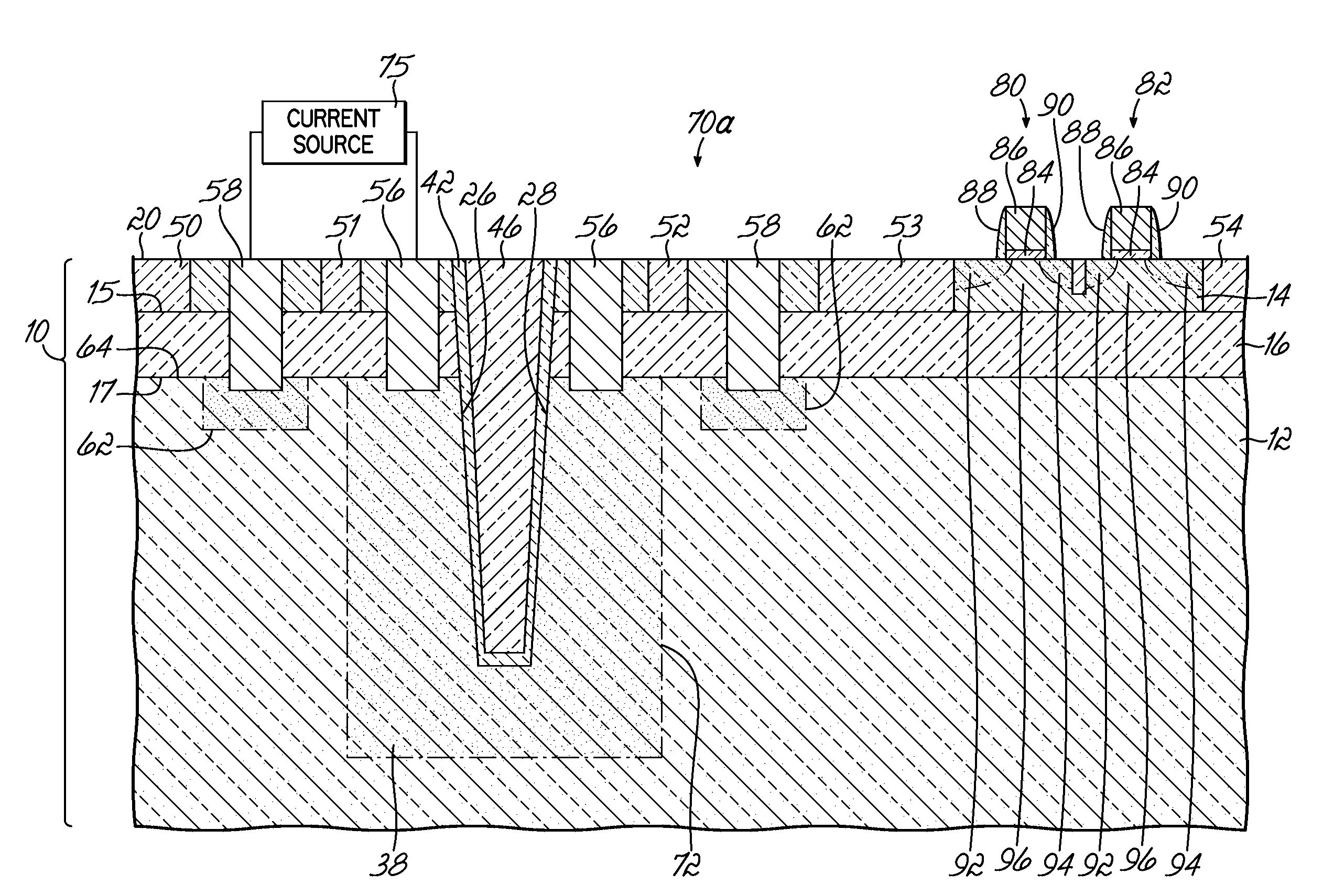
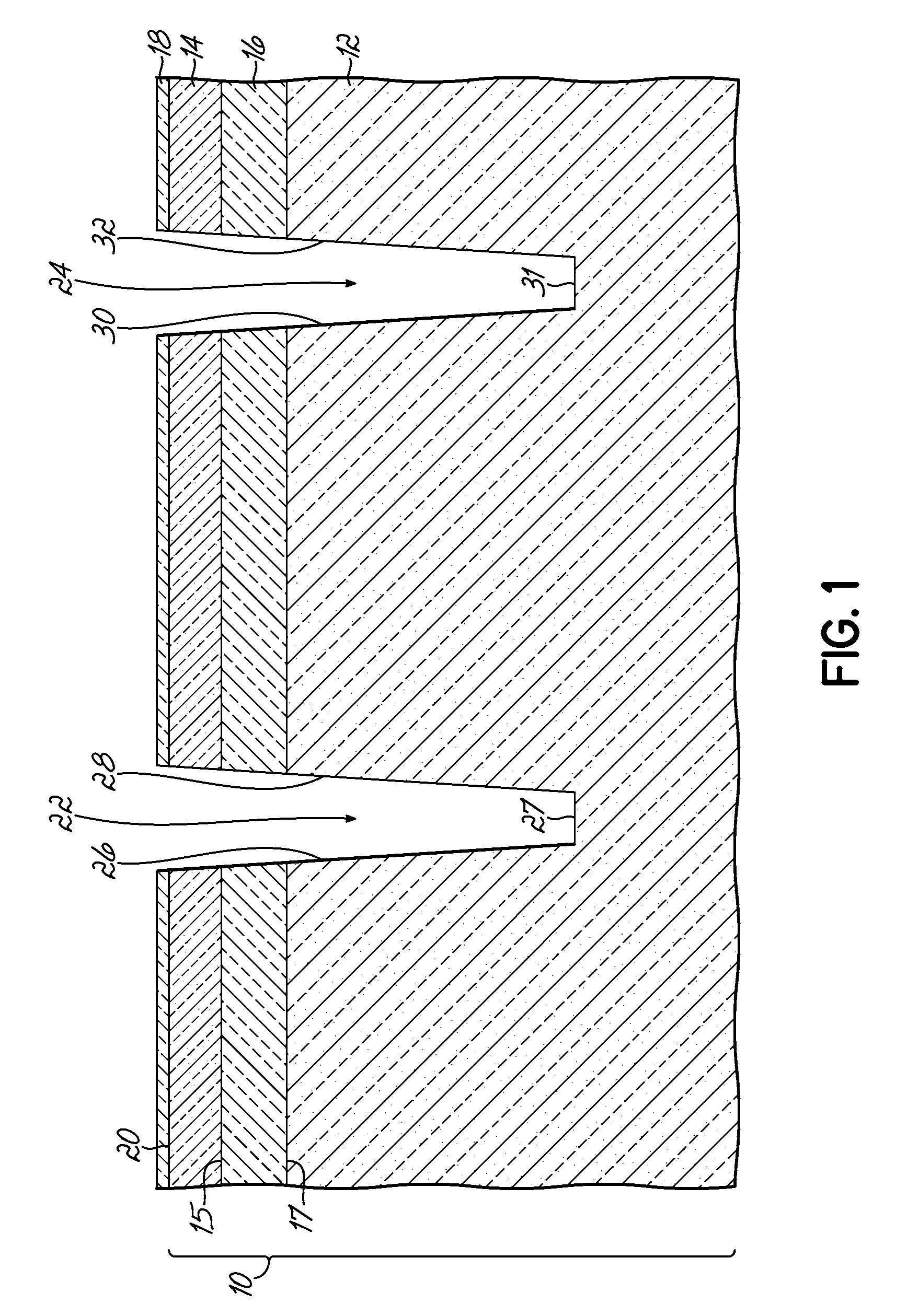
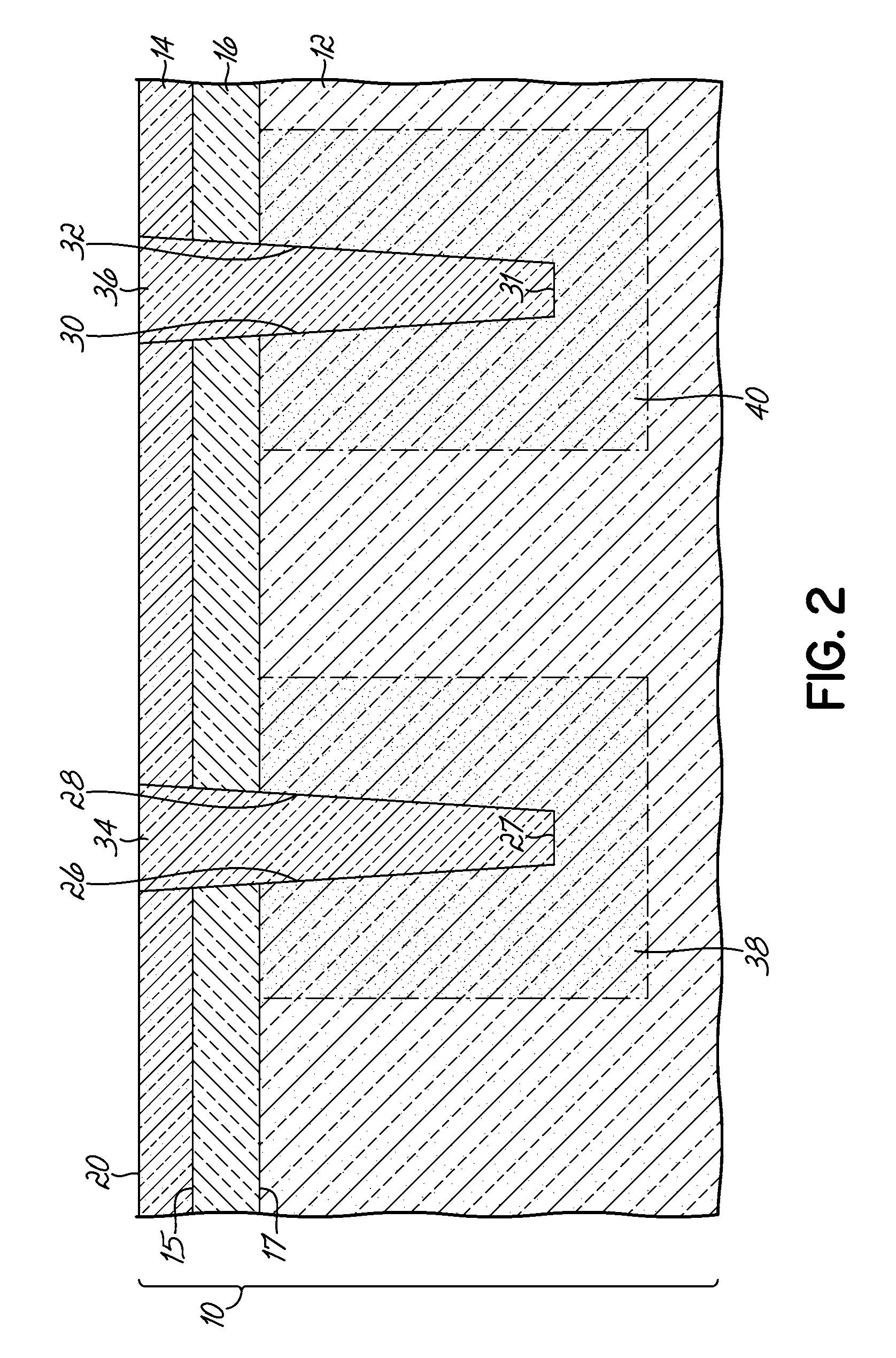
[0015]With reference to FIG. 1 and in accordance with an embodiment of the invention, a semiconductor-on-insulator (SOI) wafer 10 includes a handle substrate 12, an active semiconductor or SOI layer 14, and a buried insulator layer 16 formed of a dielectric material. The buried insulator layer 16 may be a buried oxide layer composed of silicon dioxide (e.g., SiO2). The SOI layer 14 is separated from the handle substrate 12 by the intervening buried insulator layer 16. The SOI layer 14 is composed of single crystal or monocrystalline semiconductor material, such as silicon or another material that is primarily composed of silicon. The monocrystalline semiconductor material of the SOI layer 14 may contain a definite defect concentration and still be considered to be single crystal. The handle substrate 12 may also be constituted by a single crystal or monocrystalline semiconductor material, such as silicon, or another type of material. The buried insulator layer 16 electrically isolat...


PUM


Abstract

Trench-generated device structures fabricated using a semiconductor-on-insulator (SOI) wafer, design structures embodied in a machine readable medium for designing, manufacturing, or testing an integrated circuit, as well as methods for fabricating trench-generated device structures. The device structure includes a trench extending through the semiconductor and insulator layers of the SOI wafer and into the underlying semiconductor substrate, and a first doped region in the semiconductor substrate. The doped region, which extends about the trench, has a second conductivity type opposite to the first conductivity type. The device structure further includes a first contact extending from the top surface through the semiconductor and insulator layers to a portion of the semiconductor substrate outside of the doped region, and a second contact extending from the top surface through the semiconductor and insulator layers to the doped region in the semiconductor substrate.

Description

BACKGROUND[0001]The invention relates generally to semiconductor device fabrication and, in particular, to device structures fabricated using a trench, design structures for an integrated circuit, and methods of fabricating device structures, such as bipolar junction transistors and diodes, using a trench.[0002]Bipolar junction transistors are typically found in demanding types of analog circuits, especially analog circuits used in high-frequency applications. For example, bipolar junction transistors are commonly used in radiofrequency integrated circuits (RFICs) found in wireless communications systems. Bipolar junction transistors may be combined with complementary metal-oxide-semiconductor (CMOS) field effect transistors in bipolar complementary metal-oxide-semiconductor (BiCMOS) integrated circuits, which take advantage of the favorable characteristics of both transistor types.[0003]A typical bipolar junction transistor includes three semiconductor regions, namely the emitter, ...

Claims


Application Information

Patent Timeline
IPC IPC(8): H01L29/06G06F17/50H01L21/762
CPCH01L21/2254H01L21/743H01L27/0623H01L21/8249H01L21/76283
Inventor ANDERSON, BRENT A.NOWAK, EDWARD J.
Owner GLOBALFOUNDRIES US INC
Why Eureka
Try Eureka