

Strain Si BiCMOS (Bipolar-Complementary Metal-Oxide-Semiconductor) integrated device based on SOI (Silicon on Insulator) substrate and preparation method thereof
A technology of integrated devices and devices, applied in the field of strained Si BiCMOS integrated devices and preparations based on SOI substrates, can solve the problems of confinement, low carrier material mobility of Si materials, etc.
- Summary
- Abstract
- Description
- Claims
- Application Information
AI Technical Summary
Problems solved by technology
Method used
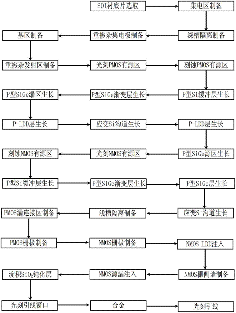
Image

Examples
Embodiment 1
[0105] Embodiment 1: The strained Si BiCMOS integrated device and circuit based on SOI substrate with a channel length of 22nm are prepared, and the specific steps are as follows:
[0106] Step 1, epitaxial growth.
[0107] (1a) Select the SOI substrate, the support material of the lower layer of the substrate is Si, and the middle layer is SiO 2, with a thickness of 150nm, and the upper material is doped with a concentration of 1×10 16 cm -3 N-type Si with a thickness of 100nm;
[0108] (1b) Thermally oxidize a layer of SiO with a thickness of 300nm on the substrate surface 2 Floor.
[0109] Step 2, isolation area preparation.
[0110] (2a) Epitaxially grow a layer with a doping concentration of 1×10 on the SOI substrate 16 cm -3 The Si layer, with a thickness of 2 μm, serves as the collector area;
[0111] (2b) Thermally oxidize a layer of SiO with a thickness of 300nm on the substrate surface 2 Floor;
[0112] (2c) In the photolithographic isolation area, a deep ...
Embodiment 2
[0161] Embodiment 2: The strained Si BiCMOS integrated device and circuit based on SOI substrate with a channel length of 30nm are prepared, and the specific steps are as follows:
[0162] Step 1, epitaxial growth.
[0163] (1a) Select the SOI substrate, the support material of the lower layer of the substrate is Si, and the middle layer is SiO 2 , with a thickness of 220nm, and the upper material is doped with a concentration of 5×10 16 cm -3 N-type Si with a thickness of 110nm;
[0164] (1b) Thermally oxidize a layer of SiO with a thickness of 400nm on the substrate surface 2 Floor.
[0165] Step 2, isolation area preparation.
[0166] (2a) Epitaxially grow a layer with a doping concentration of 5×10 on the SOI substrate 16 cm -3 A Si layer with a thickness of 2.5 μm acts as a collector area;
[0167] (2b) Thermally oxidize a layer of SiO with a thickness of 400nm on the surface of the substrate 2 Floor;
[0168] (2c) In the photolithographic isolation area, a dee...
Embodiment 3
[0217] Embodiment 3: The strained Si BiCMOS integrated device and circuit based on SOI substrate with a channel length of 45nm are prepared, and the specific steps are as follows:
[0218] Step 1, epitaxial growth.
[0219] (1a) Select the SOI substrate, the support material of the lower layer of the substrate is Si, and the middle layer is SiO 2 , with a thickness of 300nm, and the upper material is doped with a concentration of 5×10 16 cm -3 N-type Si with a thickness of 120nm;
[0220] (1b) Thermally oxidize a layer of SiO with a thickness of 500nm on the surface of the substrate 2 Floor.
[0221] Step 2, isolation area preparation.
[0222] (2a) Epitaxially grow a layer with a doping concentration of 1×10 on the SOI substrate 17 cm -3 The Si layer, with a thickness of 3 μm, serves as the collector area;
[0223] (2b) Thermally oxidize a layer of SiO with a thickness of 500nm on the substrate surface 2 Floor;
[0224] (2c) In the photolithographic isolation area,...
PUM
| Property | Measurement | Unit |
|---|---|---|
| thickness | aaaaa | aaaaa |
| thickness | aaaaa | aaaaa |
| thickness | aaaaa | aaaaa |
Abstract
Description
Claims
Application Information